MORE ON THE
COLPITTS OSCILLATOR
I have added a lot more on the Colpitts
Oscillator because a lot of the circuits on the web, claiming to
be Colpitts Oscillators, are not actual Colpitts designs,
A Colpitts circuit uses a TANK CIRCUIT to produce the frequency
and many of the web circuits are using a FEEDBACK arrangement to
produce the frequency and not the phenomenon of a TANK
arrangement.
It does not matter if you
have a tapped inductor or split capacitors, the two or three
components operate in a TANK arrangement.
I have fully explained the difference and
features of all the different arrangements and you will be able
to see the differences when looking at the circuits.
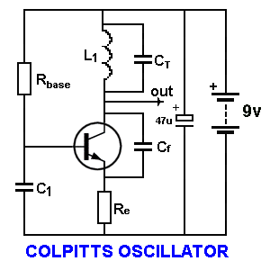
Let’s go through the main points of a Colpitts
Oscillator. The video mentions the fact that the inductor has to
be delivered energy and then this energy is transferred to the
capacitor. To deliver energy to an inductor you have to have a
strong signal with a lot current capability as the inductor has
a lot of opposition to anything trying to deliver current to it.
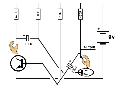
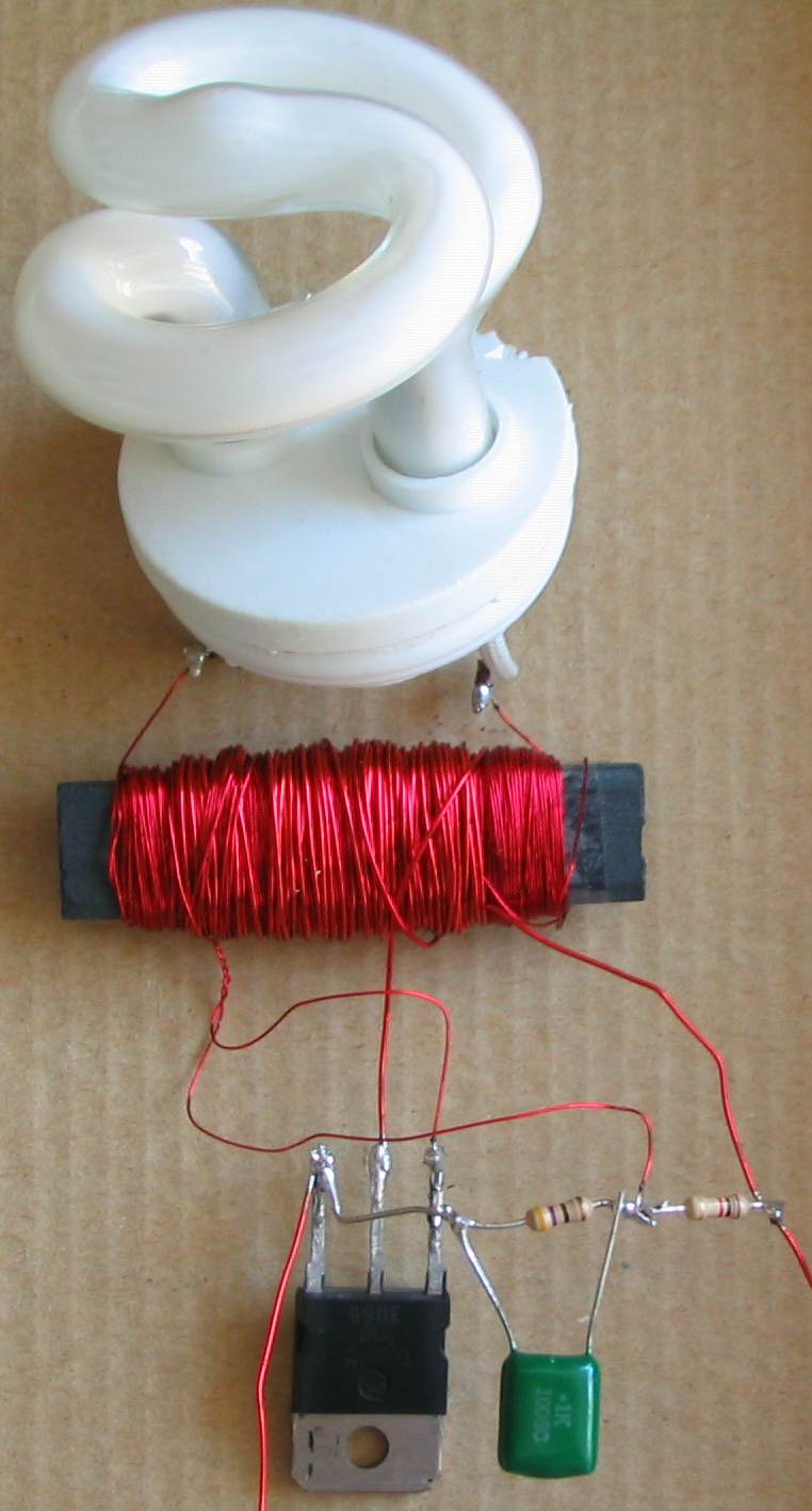
You will find a true, real, Colpitts oscillator on
talkingelectronics.com website under FM Bug. The coil is
connected to the power rail and the transistor delivers current
to the coil DIRECTLY. And the coil gets fully magnetised. The
transistor disappears from the circuit and the coil delivers its
energy to the capacitor in the opposite direction to produce a
powerful waveform that has no surrounding components to
interfere with the amazing operation called a TUNED CIRCUIT. It
produces a sine wave of known frequency and is very accurate and
stable.
None of these important features l have mentioned are present in
the circuit in this video. The inductor does not get a strong
amount of current. The inductor and or capacitor does not get
disconnected from the rest of the circuit so that it performs
its natural oscillation and because components are always
connected to these components, the TUNED CIRCUIT does not have
any “Q” factor. “Q” factor is a mark of the tuned circuit
oscillating at definite frequency that you can count on.
None of these factors are present and the circuit is just a
feeble feedback circuit with any unknown frequency of operation.
There are so many mistakes with this circuit, l could write a
book. For a start, it is not a Colpitts Oscillator, but a
feedback oscillator that works at some unknown frequency. A
Colpitts oscillator has a TUNED CIRCUIT and for a tuned circuit
to “self oscillate” it must be disconnected from the rest of the
circuit. This is achieved when the coil and capacitor are in the
collector circuit. They then give their full potential of twice
the supply voltage and have the full value of “Q.” The circuit
in this video provides none of the requirements of a tuned
circuit. Every resistor value is wrong and every capacitor value
is wrong. My circuit will transmit 29miles from the top of a
mountain on a 3v supply @ 90MHz. That’s what can be done when
you know what you are doing. Colin Mitchell.
talkingelectronics.com talking@tpg.com.au
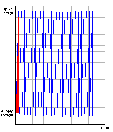
The first question you ask is where is the TUNED CIRCUIT? A
Tuned Circuit is a resonant circuit that produces a frequency by
the amazing phenomenon of passing energy from an inductor to a
capacitor and back again and the output is a sine wave.
But for this to work fully and correctly, it has to be
disconnected from the rest of the circuit. If it is still
connected,the amplitude will be less and the timing will be
longer and you cannot use the component values because of the
external influence.
Secondly, the inductor must be energised with a high current
because an inductor hates to be energised and it resists being
energised. So you need a lot of current behind the voltage you
are supplying to produce the magnetic flux.
Thirdly, you need to keep supplying voltage and current until
the inductor is fully magnetised and stops producing an opposing
voltage. This is when you know the inductor is fully magnetised.
And that’s when you know how much the tuned circuit will
transfer energy to the capacitor. In a correctly-designed
circuit, the tuned circuit tells the rest of the circuit when
this point is reached.
And now the tuned circuit stores energy. In the early days of
transmitters, the engineers were amazed that the tuned circuit
stored energy and that how it got its name. TANK CIRCUIT.
None of these features are present in this circuit and although
it will work at some unknown frequency, it is not stabilised via
a TUNED CIRCUIT but simply by feedback components.
All the Colpitts oscillator videos are fake.
They are not a Colpitts oscillator.
They are simply a feedback oscillator.
Let me explain how a Colpitts oscillator works. And in fact how
many oscillators work.
An oscillator uses an amazing feature of placing a coil and a
capacitor in either parallel or series and giving the components
a small amount of energy and one component will pass the energy
to the other and back again many times. In this process the
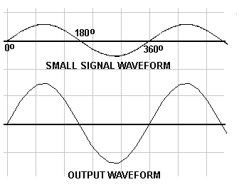
waveform is a sine wave.
This only occurs when the components are completely isolated. If
anything is connected, the energy will be lost very quickly and
the amplitude of the output will decrease.
The value of the two components determines the frequency of the
sine wave and the supplying voltage determines the amplitude.
This circuit is called a TUNED CIRCUIT and can be twice the
amplitude of the supply voltage.
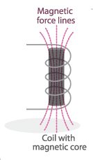
The secret in doing this is the way the coil (inductor) works.
The rest of the circuit does not determine the frequency, but it
is told when to deliver energy to the two components.
These two components are also called a RESONANT CIRCUIT or TUNED
CIRCUIT.
And the best name is TANK CIRCUIT.
One of the requirements that is never mentioned is this:
An inductor (coil) needs a lot of current to create the magnetic
flux and the supply voltage has to be high too because the
inductor produces a back-voltage that is almost equal to the
supply voltage and of you want to increase the energy being
stored by the inductor in the form of magnetic flux, you have to
keep increasing the supply as the coil keeps increasing the
back-voltage.
Eventually the back-voltage stops and you know the inductor is
fully magnetised. At this point the inductor is said to be
saturated. And any further supply of current is wasted.
The two components that create the Tuned Circuit can be in
parallel or series and the same amazing effect will occur.
The two components are connected to a circuit and the circuit
delivers energy. The two components tell the circuit to stop
delivering energy and the circuit disappears.
The two components are now allowed to create the amazing effect
of transferring the energy.
The inductor will be fully magnetised and the capacitor will be
fully charged.
They are isolated from the rest of the circuit.
A capacitor will hold its charge but an inductor will not “hold”
its magnetism.
Because the pair are not receiving any external current, the
magnetism (the magnetic lines of force) will start to collapse
and this action produces a voltage in all the turns that is in
the opposite direction.
What results is identical to placing two batteries together with
the positive to the negative. It is like a short-circuit and
current can flow around the circuit.
The magnetic flux gets turned into voltage and this voltage has
current and it discharges the capacitor. This operation takes a
long time and the waveform it produces is half a sine wave.
The inductor has used up half its energy and now it starts to
charge the capacitor in the opposite direction. The capacitor
resists charging but as the magnetic flux collapses, the voltage
it produces increases and this causes the capacitor to charge.
This takes a long time and even when the inductor is nearly out
of flux, it still produces a charging voltage. A bit like a
collapsing balloon. It still releases lots of air, right down
the final amount.
When all the flux has been converted, the value of the two
components is equal with the amount of energy they hold and the
capacitor will have a reverse voltage across it, equal in value
to the original voltage.
When you hold one end fixed, the swing in voltage on the other
end is equal to the original applied voltage.
This is due to the capability of the inductor.
This action will go back and forward with the amplitude
decreasing all the time until zero.
However the Tuned Circuit is connected to the rest of the
circuit with a small capacitor and it notifies when the first
cycle has been produced.
The main circuit then delivers a small amount of energy for the
next cycle. The point to note is this.
The main circuit has nothing to do with the time taken to charge
and discharge the capacitor.
The main circuit may not know when to stop delivering energy to
the coil and capacitor but the coil can only release the amount
according to its value. And the capacitor can only store energy
according to its value of capacitance.
That’s why you can have any powerful circuit delivering energy
and the Tuned Circuit will produce the same frequency.
The main circuit gets “cut-off” when it is doing this.
However the circuit is “voltage-dependent” or
“voltage-controlled” and a higher voltage will produce more flux
and the capacitor will charge to a higher voltage, but due to
other charging and discharging features, which we will not
cover, increasing the supply voltage has very little effect. BUT
it does have an effect.
The circuit has a RESONANT FREQUENCY. Compared to this
frequency, the supply changes are minimal, if not microscopic.
We can call this circuit: “very stable.”
Not Crystal Locked, but stable.
Now, if you have a circuit that does not directly deliver a
strong pulse directly to the inductor, the Tuned Circuit will
not work. This injection has to be very quick and it has to
inject a lot of current.
No-one has ever explained these basic points of understanding.
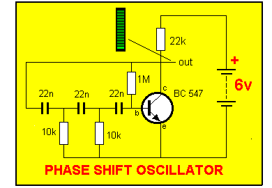
THE TANK CIRCUIT
There are 4 different arrangement that are called TANK CIRCUITS.
The real TANK CIRCUITS has a coil and capacitor in parallel.
This is the one that can be fully described and has the largest
output.
The other three have either a tapped coil, split capacitors or a
series combination of coil and capacitor.
I have already described the type l prefer, as it can be
connected to the formula for ,,,, where the output is a maximum.
That’s because the energy stored in the capacitor is equal to
the energy stored in the inductor.
And secondly the two components are separated from the rest of
the circuit to produce the magical sinewave.
One end can still be connected to the rest of the circuit, but
not both ends.
If both ends are connected, the circuit will be DAMPENED and the
some of the energy will be lost. The amplitude will be reduced
and the frequency will be altered.
In the split capacitor and coil versions, the 0v rail is
connected and this means the circuit now has a point where the
energy is removed. Even when the earth is connected to the join
of the capacitors, this point will be rising and falling of the
connection is removed.
The mid point actually rises and falls about 50% of the active
end of the circuit.
So, this arrangement works entirely differently to the two
component design.
There needs to be a lot of understanding about a resonant
circuit and a “tuned circuit.” and a “filter circuit.”
As far as the operation of these is concerned, there is a lot of
difference.
That why we have the word TANK CIRCUIT.
A Tank Circuit can be two components in series or in parallel. I
only describe the parallel arrangement.
A Tank Circuit is the ultimate circuit that produces a clean
sinewave when it receives a very short pulse of energy that is
called a SPIKE. The components in the Tank Circuit become
completely isolated from the rest of the circuit and produce a
sinewave.
You can monitor this sinewave by drawing off a very small amount
of energy but anything else will reduce the amplitude and alter
the frequency.
A FILTER is a completely different item. It may look like a
series tank circuit but if the two components are not isolated
from the rest of the circuit, it does not produce the phenomena
of an independent sinewave.
A Filter can consist of three components in the formation of the
letter “pi” or just two components.
A resistor and capacitor will have a filtering effect and an
inductor and capacitor will have a filtering effect at a
particular frequency. Some will call this filtering at a
resonant frequency or “particular frequency” or “tuned
frequency” but it is not a Tank Circuit.
A Tank Circuit uses the full capability of the inductor to
produce a waveform that is twice the amplitude.
|