The self-biased
stage The H-Bridge
There are
two ways to make a Common Emitter stage. They are called
the Self-Biased stage and the H-Bridge stage.
They both perform equally, but there are some hidden
advantages in the Self-Biased arrangement that no
“Professor,” textbook, YouTube or text book has covered.
I have used both and come to the conclusion that the
Self-Biased arrangement is the cheapest and best.
We will go through some of its advantages and show how
to design a stage using no mathematics or prior
knowledge.
Firstly, let me tell you this: all the videos and
discussions are completely wrong.
Designing a stage CANNOT be determined by mathematics as
you have no idea of the gain of the transistor as they
are all batched into groups such as 150 to 250, or 250
to 350 or 350 to 450. This is the gain of the
transistor.
But these values refer to a collector current of 1mA or
10mA and will be completely different when a higher or
lower current flows.
The second point is this. As you increase the current,
thermal noise increases. That’s why the collector
current of a pre-amplifier stage must be as small as
possible.
So, you have no idea of the gain of the transistor. And
in fact, it does not matter.
Because the gain of a self-biased stage is about 70 for
any type of transistor (and for the standard values of
input and output capacitor).
So, no matter what you do, the gain will be about 70.
But the advantage of the self-biased stage is this.
It has the least attenuation of the input signal.
In other words it has the highest input impedance.
I have sold 300,000 modules using a self-biased stage
and the result is a signal that can be amplified to a
speaker in the next room and you cannot tell if it comes
from a person or the speaker. The output perfect.
So, why hasn’t this design been covered?
That’s because none of the instructors have built a
circuit in their lives.
They are simply: “Monkey see . . . monkey do.” They have
only been taught a H-bridge arrangement. They have never
built anything.
The self-biased stage is not only simpler but it
consumes less current. And it is easy to design with no
mathematics.
When you design without mathematics, you are guaranteed
the circuit will work. You have already built the
circuit.
Mathematics tells you nothing and does nothing. It is
just the gobbledygook that comes after the invention.
The transistor was not invented by the American trio. It
was known 20 years before and its primary concept was
used by radio hams to improve the sensitivity of their
ham radios.
But they did not know what they were doing and did not
have the fine “cat’s whiskers” to get a reliable
amplification.
All this was published in ham radio magazine and the
trio just improved the physical details. Even their
first transistor had a gain less than 10.
With improved technology, this has reached about 500.
But no-one has spoken ”off the cuff” and said how a
common emitter circuit is designed.
They just plough into mathematics and leave 99% of the
viewers befuddled.
Not one student could go and build a circuit after
seeing a demonstration. It’s just mesmerism. They think
they know, but they don’t.
University teaches you nothing. It’s called the
three-card trick. You think you can pick the joker, but
you can’t. You think you can learn from a University
Course, but you can’t.
You can’t because the lecturer does not know himself!
It’s called: “The blind leading the blind.
No-one questions their qualification because they have
spent $70,000 and hope it has delivered something.
But, in reality, electronics is done in a completely
different way to text books.
In fact, electronics is done in reverse.
If you want to design something, you have to study all
the available circuits and either build them or work out
which features are the best.
You cannot design something from the start. You do not
know the hidden problems.
And to prove this, l have presented hundreds of faulty
circuits from the web in my article: SPOT THE MISTAKE.
So, how do you design a Self Biased Common Emitter
Amplifier?
You need a breadboard and some components.
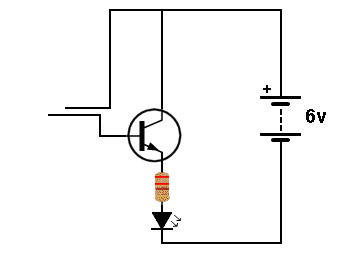
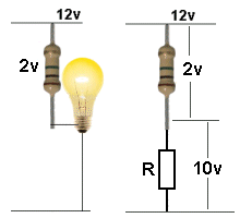
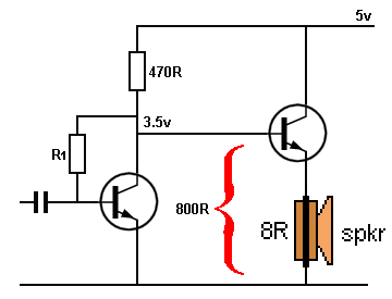
The first thing to understand is this. The aim is to get
half-rail voltage on the collector.
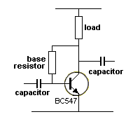
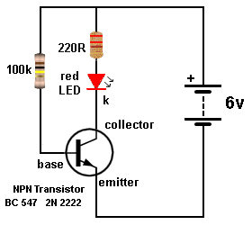
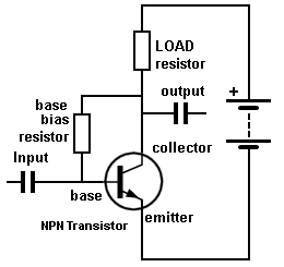
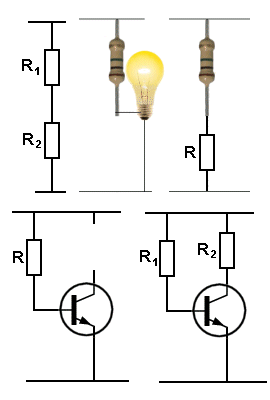
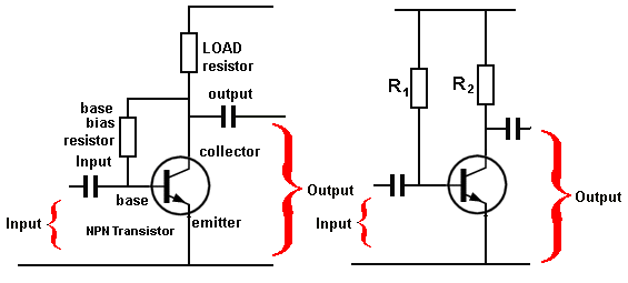
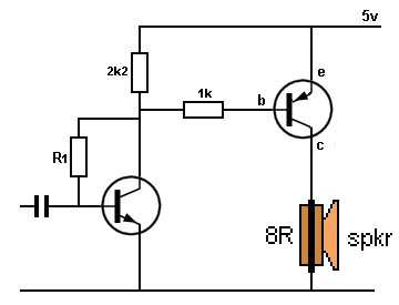
Look at the circuit. It has just 3 components. The
transistor, the collector resistor and the base-bias
resistor.
The supply voltage does not matter. You can have a
voltage as low as 3v. Any voltage above 5v will simply
take more current (wattage). If you are using a voltage
higher than 3v, increase the collector resistor by 10k
for each volt.
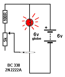
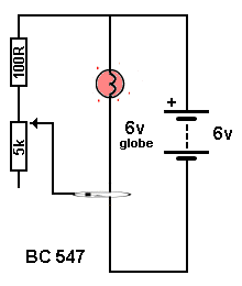
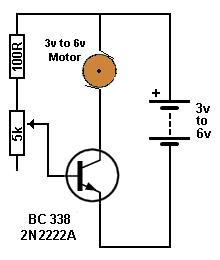
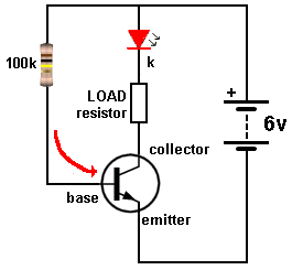
Fit the transistor and a 22k collector resistor plus 3M3
for the base resistor.
Now measure the collector voltage.
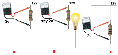
Here is a very clever trick.
Your multimeter may load the circuit if it is an
analogue meter, so change the leads to ACROSS the load
resistor. You will get two different readings and the
actual reading will be between the two.
If the reading is too low, increase the base resistor.
That’s all you have to do.
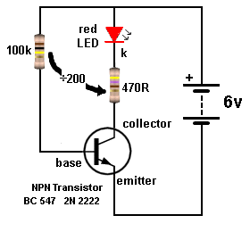
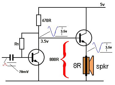
Now put 10n to 22n on the base to become the input
capacitor and 100n to 1u on the collector to become the
output capacitor.
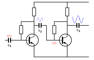
The stage is fully designed.
Add a second and third stage or connect the preamplifier
to an audio amplifier and an electret microphone to the
input capacitor with 47k load resistor.
This will give you the cleanest, loudest sound.
If you don’t believe the result, change each and every
component with half or double the value and see if it
makes any difference.
No mathematics, no frustration, just accuracy. It works
because you can see and hear it.
Everything else is just guesswork and “maybe.”
You can now try the H-bridge circuit and see if is
better and takes less current.
Now you know how you have been fooled. The self biased
stage is simper, cheaper and better.
A $70,000 University course is not be the answer. The
answer is to “teach yourself.”
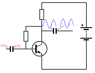
Why is the stage-gain
only 70?
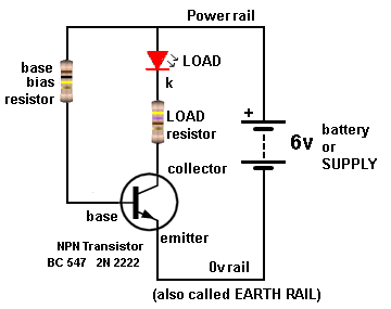
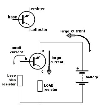
The base resistor is placed between the base and
collector and it becomes a FEEDBACK RESISTOR.
What happens is this.
When you turn on the supply, the voltage immediately
goes to the base and turns on the transistor harder than
normal and this makes the resistance between the
collector and emitter terminals of the transistor very
small and the voltage on the collector reduces to a very
low value. This is too low to operate the transistor and
the transistor turns OFF a small amount and the base
receives some voltage and a small current flows into the
base. This keeps happening until the transistor turns
OFF and OFF until the voltage on the collector is able
to supply enough current to the base to create
equilibrium where the collector voltage is half rail.
This half rail is due to you selecting the right base
resistor.
If we add current to the base via the input capacitor,
(this is when a signal is applied to the stage) the
transistor will turn ON more and the collector voltage
will fall. The collector voltage is supplying some of
the base current and now this current is reduced. This
means the transistor is modifying (reducing) the
strength of the signal and this is called NEGATIVE
FEEDBACK. In other words it is “cleaning up” the signal
and improving its “quality,” while at the same time
reducing it.
When you have a transistor with a higher gain, the
collector voltage will be lower and you need a larger
resistor for the base to get mid rail voltage.
When a signal is applied to the circuit, the same
feedback effect applies as above but this time the
resistor has a larger value and so a change in collector
voltage passes a weaker feedback to the base and this
negates the effect of the higher gain.
The end result is all circuits produce about 70 times
the amplitude of the input signal.
The base-bias resistor “kills” the gain of the
transistor as it works in opposition to the signal,
creating a larger output waveform, and lowers (reduces)
the output signal.
It is the value of the base resistor that equalises or
“marries” or reduces the gain of the transistor.
All you have to remember is this: Reduce the value of
the base resistor to reduce the collector voltage. In
other words the smaller resistance on the base turns the
transistor ON more. This makes sense because no resistor
will put full rail voltage on the collector and a very
low value will put 0.7v on the collector.
If you find any location where the instructor has
included any of the interesting and important points l
have covered in this article, let me know. I would like
to know if anyone has the slightest knowledge of how to
design a circuit.
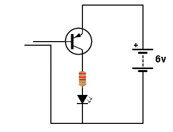
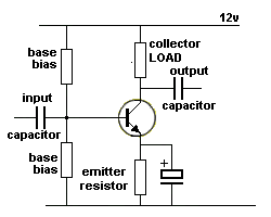
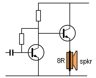
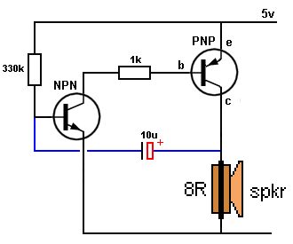
I have identified the two circuits as “self biased” and
“H-bridge” as the H-bridge is not actually self-biased
as the base resistors set the voltage on the base and
the transistor turns ON. Current flows in the emitter
resistor and produces a voltage across this resistor.
The emitter voltage increases very rapidly and starts to
turn the transistor OFF. It turns OFF more and more
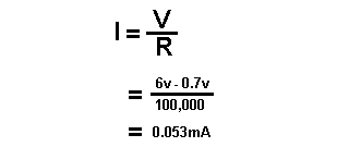
until the voltage between the base and emitter is
exactly 0.65v This is the point where the transistor is
fully turned ON.
Now the current through the emitter resistor is also
flowing through the collector resistor and it produces a
voltage across this resistor. If the voltage across this
resistor is exactly half rail voltage, you have chosen
the right values for the base bias resistors and the
emitter resistor. Otherwise you will have to change one
or more of the 4 resistors.
If you change the transistor for one with a higher gain,
the transistor will turn ON more and the collector
voltage will reduce. This will allow a higher current to
flow in the collector resistor and also in the emitter
resistor. The emitter voltage will rise and the voltage
between the emitter and base will reduce. This will turn
the transistor OFF slightly and bring the conditions to
the same as the previous lower-gain transistor. In this
way the circuit is self-adjusting.
We have mentioned that the gain of the stage is about
70.
This value is heavily dependent on the value of the load
. . . . the resistance of the input of the next stage.
We are assuming this is an ideal value and even when it
is ideal, only about half the amplitude of the signal is
delivered to it.
As we have mentioned in another article, the transistor
does not deliver the signal to the next stage. The
collector resistor delivers the signal.
Suppose we have an ideal example of 22k for the
collector resistor and 22k for the input impedance of
the stage that follows.
These two components form a voltage divider and when the
transistor is turned OFF, the voltage at the mid-point
cannot be higher than half-rail voltage. So, this is a
maximum, and will be less due to the voltage across the
coupling capacitor. When the transistor turns ON, it
simply turns OFF the next stage and no energy is
delivered.
That's why you cannot make any predictions, and all the
YouTube videos fall down by making wild claims and not
including the impact of the things we have mentioned.
Why do l recommend the self biased
stage?
The H-bridge has base-bias resistors and these can
reduce the input waveform by 50% so the stage has to
work harder to get the same results as the self-biased
arrangement. This is about the only major difference.
All the other losses will be the same. |

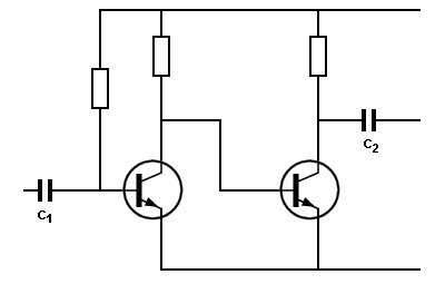

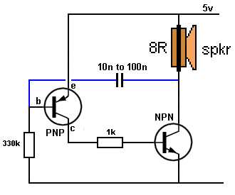
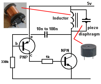
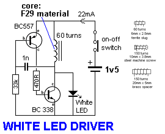
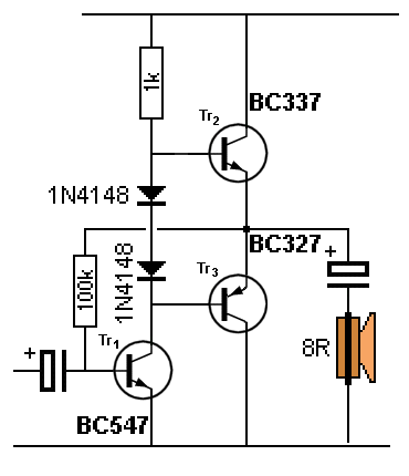
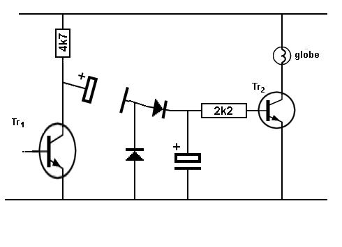
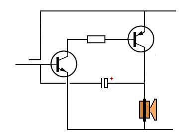
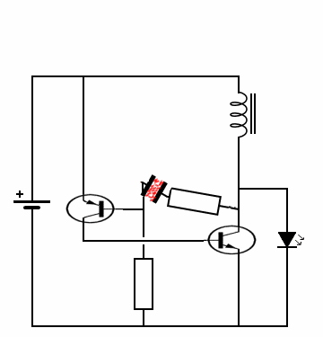
 The main difference between this circuit and the two circuits
above is the use of a single winding and the feedback to produce
oscillation comes from a 1n capacitor driving a high gain
amplifier made up of two transistors.
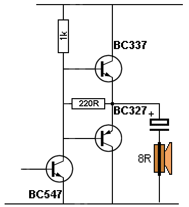
The main difference between this circuit and the two circuits
above is the use of a single winding and the feedback to produce
oscillation comes from a 1n capacitor driving a high gain
amplifier made up of two transistors.