SPOT
Page 1
Page 2
Page 3
Page 4
Page 5
Page 6
Page 7
Page 8
Page 9
There is only one thing I regret with Talking Electronics website.
The one thing I liked about Radio Shack (Tandy) was the "Lifetime
Guarantee" they provided for their products.
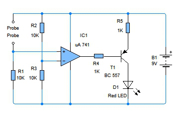
PLANT WATERER
The circuit
above is the original design. It works but it is very complex and
the op-amp takes current all the time.
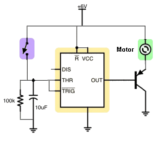
The circuit can be simplified to two transistors and 3 resistors. It takes less
than 9 microamps when "sitting around."
Spot the Mistakes
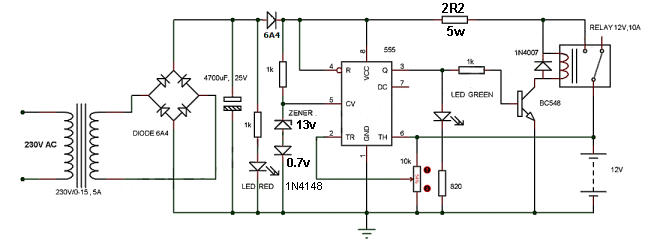
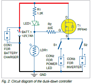
AUTO BATTERY CHARGER
This is not a faulty circuit but the simplest Automatic Battery
Charger circuit you can get.
HUM
Suppose the hum is the voltage between 13v and 15v. If we use the
voltage up to 13v, we will not get any hum.
The 10R and 2u2 will have a small effect on reducing the hum and the
emitter will deliver the improved waveform to a 68R and 220u filter. But
the voltage at the join of these two components will drop when a load is
applied and this is not a good design for a power supply.
The third circuit combines the first two circuits and adds a zener diode
to deliver only the voltage below the ripple. The voltage below the
ripple is perfectly smooth.
AMPLIFIER
The circuit has no supply rail.
The diode does nothing and been removed. The supply rail has been added.
IR DETECTOR
Look at the block diagram.
PHONE CHARGER
I don't know what this circuit is supposed to do but it will not work.
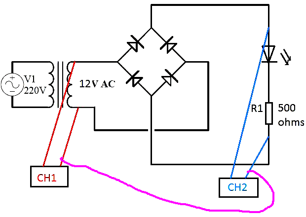
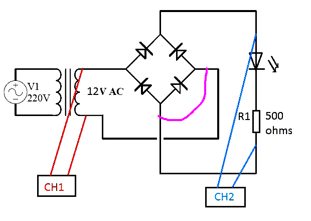
CRO PROBLEM
A reader is testing a power supply with a dual-trace CRO and placing the
probes as shown:
When the power supply is turned ON, one of the diodes is damaged.
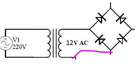
The earth lead on the probe for Channel 1 is connected to the earth lead
on Channel 2 and the purple line on the diagram above shows this.
The diagram above shows the "short circuit" on the power supply due to
the two probes.
The diagram above shows the "short circuit" puts a singe diode across
the incoming 12v AC and the diode presents a "short circuit"
when the voltage is emerging in one direction and will be
damaged. When the voltage is emerging in the other direction, the diode
is reverse-biased and nothing happens, but when the voltage reverses
again, a very heavy current flows.
This is just one of the dangers of connecting two probes to a
circuit.
COUNTER
If the 100k pot is turned fully clockwise, the pot and the transistor
will blow up.
TRANSISTOR TESTER
Look at this PNP circuit:
The transistor is connected AROUND THE WRONG WAY !!!!
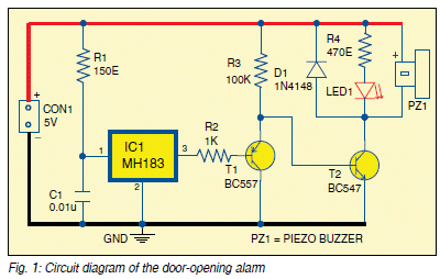
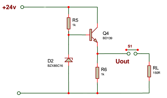
HOME ALARM
The circuit contains a fundamental mistake.
OVER VOLTAGE CUT-OUT
THE MISTAKES!
Page 26
Page 10
Page 11
Page 12
Page 13
Page 14
Page 15
Page 16
Page 17
Page 18
Page 19
Page 20
Page 21
Page 22
Page 23
Page 24
Page 25
Page 27
Page 28
Page 29
Page 30
![]()
It should have been in the form of an encyclopaedia.
I have produced so may "pearls of wisdom" and answers to circuit
problems that the website is one of the largest on the net.
And it is different to any other website or text book.
It answers all those questions left unanswered after a lecture or after
reading a text book.
So may times I have read a text book and said " I don't
know what he is trying to say!"
Everything could be made clearer by including two or three circuits or photo's. But in many cases the author has never
built the circuit and tested it.
The biggest mistake a beginner can make is thinking a text book will answer
his questions, solve his problems or teach him electronics, or a course will enable him to become a technician.
A current Masters of Electronics course in Australia runs for 4 years
and in the first three years the students have done little or no
soldering, and only worked on a very poorly produced PC board for an AM
radio.
Their final project is to produce a robot that finds and picks up pucks.
I don't know how many pre-made modules are allowed or if a
whole Robot can be bought off-the-shelf, but how is a student going to design and
produce a robot with steering, detecting a puck, picking it up, two-way
remote control, camera-detection and programming a microcontroller, in 6 months.
No-one with less than 2 years ROBOT ENGINEERING and hundreds of projects
under his belt, could come up with a project like this.
It just shows the absurdities of University teaching.
They think you can come out of the course with all the capability of designing a robot
for the Moon Lander, after a single project; while in reality the student can barely desolder a 40 pin
IC.
![]()
After helping 4 electronics forums for the past 3 years, I can say the
actual basic understanding of electronics of those who have been in the
industry for up to 40 years, is quite lacking.
Yes, many of them have carried out research, repaired thousands of
pieces of equipment or worked in electronics at the hobbyist level, but
some of the replies and answers to readers questions contain
fundamental, glaring, errors.
I don't know everything about electronics but I have certainly covered a
lot of the basics and explained things that have never been covered
before.
And it's only when you cover a circuit in minute detail that you can
explain its operation.
It's only when you can "SEE A CIRCUIT WORKING" that electronics comes
alive and you can actually work on the circuit to improve its
performance or alter its characteristics.
The next stage in the development of the web will be to produce
interactive discussions with circuits that "move" and show the capacitor
charging and the transistors turning ON and the IC's carrying out a
function.
This can come with short videos showing the circuit working and include
the sound.
Some of the simulation software already shows "electrons" moving around
the circuit but none actually show the resistor limiting the current or
the capacitor charging or the transistor turning ON.
![]()
I don't know what a Lifetime Guarantee means but the concept infers that
any problem will be addressed and fixed.
The stores were a very poor example of an electronics component supplier
and they lurched from one decade to the other with a few successful
products such as stereo amplifiers, CB radios, loud hailers, 200
electronics experiments kits, Gold Detectors, computers and then
everything died.
But the concept of a guarantee still stays in my head and for anyone who
has bought a kit from Talking Electronics and not been able to get it to
work, the policy exists to be able to send it in for checking and repair
at no cost.
Some readers have bought $200 worth of kits and are not heard-of again. To get
all the kits working will require a lot of skill and since many were
beginners, they should have contacts us for assistance.
It's no good giving up and letting anything rest as you only begin to
learn electronics when you have found and fixed a fault.
I have fixed over 26,000 black and white TV's and if I gave up after a few
minutes, almost none of the sets would have been fixed.
Sometime it takes hours to locate a fault and something it is just
replacing a cracked valve.
But dogged determination is the only attribute you need to see your way
through a design . . . to eventual completion.
It would be wonderful if everything was easy and straight-forward.
But that means the product and idea would already be on the market.
New ideas take skills that have not yet been tested and and since
everyone's brain has an endless capacity for invention, new ideas and
products will come on the market all the time.
It's just your aim to make that new product . . . yours !!
![]()
Another circuit
from
Professor Mohankumar. The probes are placed in the soil of an
indoor pot-plant and the LED comes ON when the soil dries out.
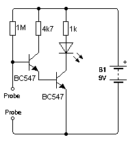
When ever you design a circuit, look on the web to see how it has already been
designed and ask yourself if any of the components can removed and if the
circuit can be simplified.
![]()
No text book and NO project in a magazine has ever included a section "
And how wrong they are.
There are so many variables to making a circuit.
Many projects are just on the verge of not working and by using a
different transistor or a different component or even a different
layout, the circuit fails to work.
I have already given examples of poorly deigned multivibrator circuits
that I could not get to operate and others that stopped working as soon
as the voltage dropped a few volts.
That's why I consider these pages one of the most important additions to
the website.
You can learn 10 times faster from other people's mistakes than dragging
yourself through the theory of the circuit.
I have proved this with 2 apprentices who came "off the street" and were
fixing black and white TV's after 2 - 4 weeks of watching what to do.
Of course you can go the "theoretical route" but this route will have
much more significance if you have already experimented with the
circuits and seen what effect is produced when components are changed.
And you have a much better "grass roots" understanding.
![]()
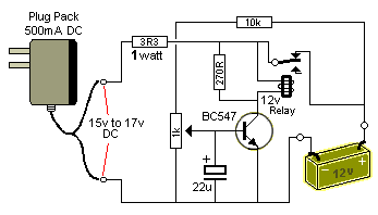
It is so simple, that no one believes it will work.
It is mainly designed to keep a battery topped up in a car, motorcycle,
snow-plough, etc stored in a garage for a number of months.
A battery loses energy at the rate of 10mA to 100mA, depending on the
battery and the temperature and the age of the battery and you need to
keep adding this energy to keep it charged.
This circuit will not overcharge the battery because the charging current
is less than 500mA and the current is turned off when the battery
voltage reaches 13.7v.
Read the full article: Automatic
Battery Charger and you will see how the circuit works. It is quite
complex.
![]()
Hum is the background noise you hear in an amplifier when the
volume is turned down.
It comes from the power supply where the diodes charge a set of
electrolytics from the alternating current (AC) from the "Mains."
The Mains is called the "AC."
If the Mains has a frequency of 50Hz, the power supply produces 100Hz
hum and if it is 60Hz, the frequency is 120Hz. This is because the
bridge delivers the waveform from the 0v axis to the peak of the
waveform to the output and at the same time it inverts the wave (from
the 0v axis to the negative peak) and places it between each of the
positive portions of the wave and this effectively doubles the
frequency.
Hum is the ripple at the top of the voltage coming from the power
supply: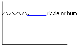
Here are 3 circuits and we will explain how well they perform.
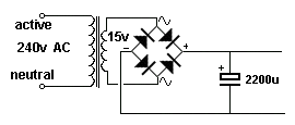
This circuit will deliver all the hum to the load. If the load is an
amplifier, the background will hum.
It delivers the full voltage from the power supply, including the HUM
component.

This circuit will deliver some of the hum to the load.
The voltage is delivered (including the hum component) and
the hum component is reduced slightly by a process called SMOOTHING.
The output voltage is reduced by a process called ATTENUATION.
But the hum is not REMOVED.
There are two faults with this circuit.
The transistor increases the effectiveness of the 2u2 by 100 times, so
why not make the 2u2 larger.
if it is 220u, it will effectively be equal to 22,000u and provide very
good hum reduction.
The 10R should be increased to 220R to improve the effectiveness of the
220R/220u combination.
The 68R will lower the output voltage and at 100mA current, the output
will drop 6.8 volts !!
Obviously, this is not a very good circuit.
The zener and 220u creates a very stable 12v6 and this is fed to the
transistor. We could use this stable 12.6v and feed it directly to the
load but as soon as we require more than 100mA, we will be taking all
the current from the zener and the output voltage will drop.
At the moment the supply voltage is about 18v from the bridge rectifier,
and this creates 5v across the 47R. The current through the 47R is about
100mA and this current flows through the zener.
This is the maximum current we can use and if we take say 120mA, the
zener DROPS OUT OF REGULATION and the voltage across it drops to a lower
value. So, we can NEVER take more than 100mA from the
stabilization-section of the circuit - the zener diode.
The transistor has a gain of about 100 and theoretically we can take 100
times 100mA (=10Amp) but the power supply will not deliver this high
current so with a current up to 1, 2 or 3 amps, the output voltage will
be fully stable. (The bridge and transistor are 3 amp
devices.)
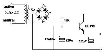
The final circuit using a zener and transistor to
provide a stable
output voltage, with the hum removed.
![]()
Another useless circuit
from
Professor Mohankumar.
The circuit is absolutely USELESS.
The only time when the circuit acts as an amplifier is when the input
voltage is between 8.2v and 8.4v.
At all other times the amplifier is turned OFF or fully saturated.
Where can you get a signal containing audio information between 8.2v and
8.4v ???
Another untried, untested, useless circuit from an Indian "Professor."
![]()
Another useless circuit
from
Professor Mohankumar.
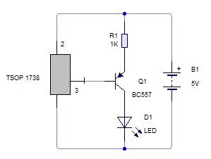

When the output transistor is OFF, pin 3 is HIGH and the BC557
transistor is not turned on. The LED does not illuminate.
When the output transistor is ON, the voltage on pin 3 is about 0.3v and
the base of the BC557 transistor will be 0.3v above the 0v rail.
The emitter of the BC557 will be 1v above the 0v rail and the collector
will be 0.8v above the 0v rail.
The LED will not be turned on.
The LED will NEVER be turned ON !!!
Another untried, untested, useless circuit from
Professor Mohankumar.
Where does he get this rubbish from????![]()
Another useless circuit
from
Professor Mohankumar.
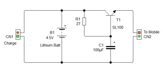
The output of the circuit is 3.8v as 0.7v is lost across the
base-emitter junction of the transistor.
A mobile phone needs 5v because it has a protection circuit and also a
current limiting (called the charging circuit) between the input and the
battery.
The battery is 3.6v and if the input voltage is 3.8v, NO CHARGING WILL
OCCUR.
This circuit simply WILL NOT WORK.
![]()
In the circuit above, the voltage emerging from the transformer is
classified as "above earth" (this can also mean "below earth") and means
the voltage is not an "EARTH POINT."
The other point is not strictly an EARTH POINT but we have made it an
earth point by connecting the earth probe.
In all circuits and PC boards that have an "earth plane" or "ground
plane," this trace or track or plane is not necessarily "earth" as it
may have no connection to the earth pipe of your house via any wiring.
But as soon as you connect the earth probe of a test probe to the track,
it becomes EARTH via the CRO.
This is now your reference point for all other voltages.
This is very important to remember when you have hum problems with an
amplifier, especially when you are designing an amplifier and connecting
it to a power supply.
![]()
Here is a counter circuit with a number of mistakes.
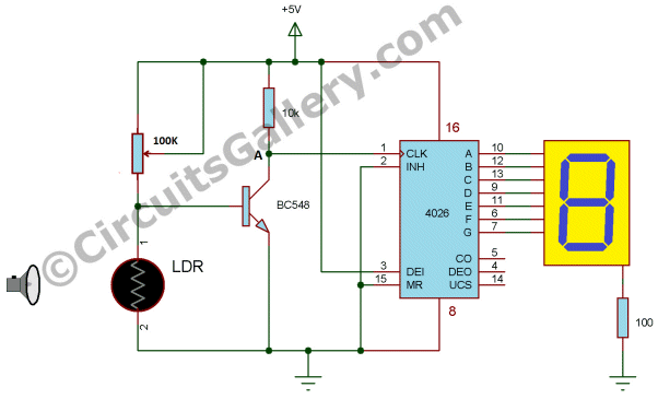
The circuit has no debounce and the count may increment by an unknown
number if the LDR receives varying light intensity.
The display will dim on the figure 8 due to the 100R in the "common"
line. As more segments are lit up, the voltage across the 100R increases
and each segment will pass less current.
![]()
Here is another INDIAN website for beginners. It is filled
with mistakes:
http://www.circuitsgallery.com/2013/12/transistor-tester-circuit.html![]()
![]()
Here is another circuit from the INDIAN website: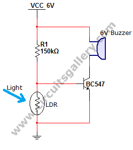
The transistor effectively reduces 150k by a factor of 100 or 200
as this is the gain of the transistor.
The 150k becomes 1k5 or 750 ohms in series with the 6v buzzer.
This means the circuit will pass between 4mA and 8mA.
The buzzer will not be very loud.![]()
Here is another circuit from the same INDIAN website:
The 6v2 zener is not needed. Here's why:
The circuit is detecting the voltage on the power rail and when it rises
too much, Q1 is turned ON and Q2, Q3 are turned OFF.
The rise in voltage on the power rail is passed to the base of the first
transistor via a voltage divider made up of R1 and R2 and through a 6v2
zener.
The pick-off voltage from the 10k will be about mid-rail voltage and
this means for every 2mV rise in the supply voltage, the pick-off
voltage will rise 1mV.
The voltage drop across the zener is not fixed. When the current is very
small the voltage across the zener is less than 6v2 but it an unknown
value and it will rise slightly as the current increases.
This means it will take a few mV rise on the power rail for each mV
increase on the base.
If we remove the zener, the pick-off voltage will be about 0.7v and this
means it will take about 20mV rise on the supply rail for each mV rise
on the base.
However the circuit does not need to detect very small rises and it will
be quite acceptable without the 6v2 zener.
It's only when you need a very close detection of the rise on the power
rail that the zener has an advantage.
I have mentioned a lot of "ratios" (detection voltage compared to rail
voltage rise) and you need to understand how and why this information is
important. Email Colin Mitchell
and I will write an article on it.
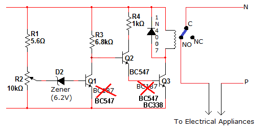
BC187 is a PNP transistor !!
Always use BC547 for a standard NPN transistor as this indicates the
cheapest, lowest-voltage, lowest-current transistor can be used.
If you want a higher current, specify BC338. This makes the circuit easy
to interpret.
The 1N4007 diode is not needed as the output transistor turns ON and OFF
so slowly that the relay does not produce any back EMF.
These are points that show the author of the circuit does not know much
about electronics.
![]()
HIGH WATER AND LOW WATER
ALARM
Here is another circuit from the same INDIAN website. The
alarm sounds if the water is low or overflowing.
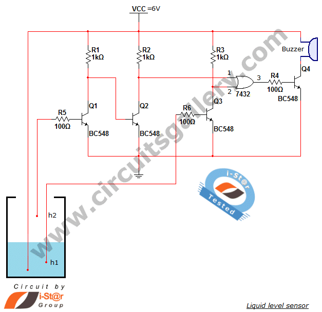
The circuit can be simplified and the OR
gate can be removed.
The
skill in designing a circuit is to make it as simple as possible, and
work out if each component is needed. You don't "add an OR
gate" just because the circuit needs a gate. See if you can design
around the need for a gate and try diodes or resistors to provide the OR
function.
BATTERY CHARGER
Another, untried, untested faulty design.
There are lots of ways of including an OR gate without using a digital
gate. You can use transistors, diodes or resistors.
The following circuit uses resistors so the output transistor can be
driven from two different transistors: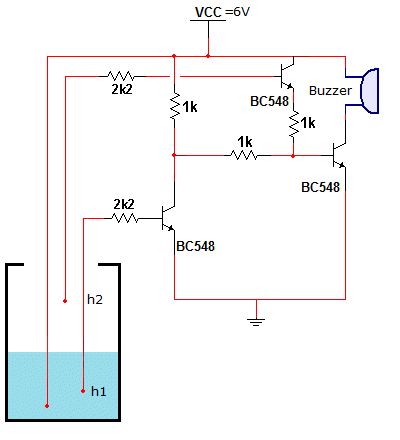
![]()
Here is another circuit from the same INDIAN website.
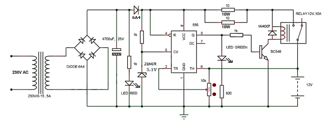
Pin 5 and 6 are effectively at
the same potential via components inside the 555 if nothing is connected
to pin 5.
Let's state this a little more accurately.
Pin 5 is at 66% of rail voltage via three 5k resistors inside the chip.
If pin 6 rises slightly above this voltage by a few millivolts, the chip
effectively "turns OFF." Output pin 3 goes LOW.
Pin 6 can be designed to detect any voltage by "injecting" a particular
voltage into pin 5.
The circuit show a 5v1 zener on pin 5, but if this zener is 13v (plus an
ordinary diode of 0.7v) the detection voltage for pin 6 can be set at
13.7v.
The 10k pot on pin 6 can then be adjusted to 12v for the lower value to
turn the 555 ON.
The maximum voltage from the bridge will be about 20v.
The battery voltage will be about 13v. The difference is 7v.
As soon as 1.4amps flows through the 10R / 10R the voltage drop will be
7v and it is pointless having a 5 amp transformer and bridge.
This is another circuit that has never been tested.
Hashem Pakdel
hashempakdel@gmail.com pointed out the fact that the maximum
voltage for the 555 is about 16v to 18v. It will
BLOW UP in
this circuit
DO NOT TRY THIS CIRCUIT.
ooooo00000ooooo
Here is another battery charger circuit that
has never been tested.
The 100R feeding the battery will only allow about 50mA of
charge-current. At 50mA, the voltage across the 100R will be 5v and Q1
will already be fully turned ON to reduce the current, so in effect the
charge currentt will be less than 50mA !!!!
The 11v zener activates Q1 at about 13.5v and at 50mA the battery only
has to rise to 8.5v and the charging current drops below 50mA.
470u in the power supply is going to produce
5v ripple. This means the charger is going to provide pulses to the
battery, but that is not a problem.
EMERGENCY LAMP
There are so many mistakes with this circuit that it will not work AT
ALL.
POWER SUPPLY
The 225 capacitor will deliver 150mA and the 100R's
will dissipate 0.15 x 0.15 x 100 = 2.25 watts.
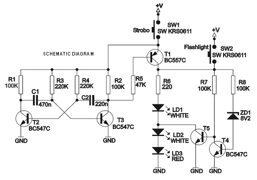
LED STROBE LIGHT
The second circuit shows how to produce a simple AND Gate with a
resistor and diode. The transistor only conducts when BOTH lines are
HIGH. It uses only half the components and saves a transistor.
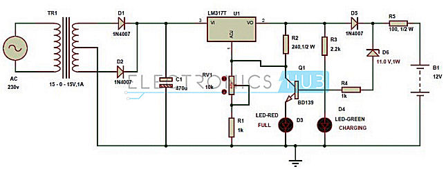
BATTERY CHARGER
Here is his article. Can you see his mistake?
CAR ADAPTER
The circuit does work if you change a few values.
BATTERY CHARGER
The biggest HIDDEN danger with this type of circuit is this:
THE ZENER DIODE
Replace the 100R with 2R2 or 3R3 and the circuit will charge the
battery.
![]()
Here is a circuit from an INDIAN website.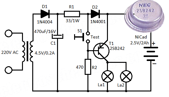
The two lamps are 2.5v torch globes and each will take about 100mA to
250mA.
The current through the 33R will be 2.5/33 = 75mA MAX.
The circuit is half-wave so the average current will be 75/2 = 38mA (or
something near this value as the 470u stores some energy that will
increase the average value).
The transistor is turned ON all the time and the globes will take
between 200mA and 500mA.
The charging current is 38mA so you can work out how long the 2Ahr
battery will last.
The test switch just turns OFF the lamps !!!
D2 is not needed as the battery will not discharge via the secondary
winding when the power fail due to the presence of D1.
Why is D1 a 400v diode and D2 a 50v diode ??
2SB242 is a GERMANIUM PNP transistor. Where are you going to get
this transistor ??????
I don't know what the author is trying to do but it is obvious the
circuit has never been built or tested.
The circuit was taken from Alok Kumar website:
https://plus.google.com/+alokkumar-NSIT/posts![]()
Here is another circuit from Alok Kumar.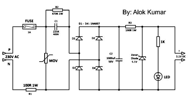
The 1watt resistors will BURN OUT !!!!
The output will deliver 5v1 and maintain this voltage as long as the
current is less than 140mA.
The 1,000u is in the wrong place to have the best effect. It should
be after the second 100R, across the 5v1.
The 100R and zener create a REGULATED 5v1 POWER SUPPLY capable of
delivering up to 140mA and the voltage will be very smooth with the
1000u across the zener.
The 1,000u WILL have an effect before the 100R, but its effect will be 100 times
greater when it is placed across the zener.
![]()
Here's a circuit
from
Professor Mohankumar. He does not know how to produce a simple AND Gate: 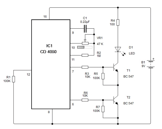
![]()
Here is another circuit from Alok Kumar.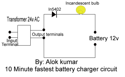
Components Required:
1. One rectifier diode IN5402, or IN5408.
2. One incandescent bulb, having nearly exact voltage rating as the
battery but current rating of the bulb should be 1/10 of the value of
battery AH (AmpereHour).
3 One transformer having double the voltage rating of the battery. For
12 v battery we need 24v Ac transformer, and current rating of 1/10 of
the AH of the battery. For 7AmpHr battery we need 7/10 = 0.7A or 700mA
current from transformer.
When we switch on the power, the diode from the transformer will produce
half wave 24vdc at output.
The incandescent bulb after the diode acts as a "voltage shocker" or a
peak voltage remover. The bulb absorbs the peak voltages and provides an
output voltage to the battery.
His BIG mistake is FASTEST BATTERY CHARGER CIRCUIT.
He has used a very small transformer and is using half-wave. It will
take at least 14 hours to charge a battery. In 10 minutes the battery
will receive very little charge.
The output of the transformer will be over 24 + 12 = 36v and the current
delivered to the battery will be fairly high. But this is for each half
cycle so the average will be about 700mA. It depends on how the globe
reacts to the voltage and current flowing in the circuit.
![]()
Another circuit
from
Professor Mohankumar: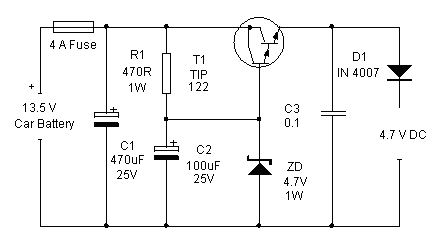
But the main point of this discussion is to ask: "What is purpose of
each component?"
A car battery is very stable as far as ripple is concerned and the 470u
will have no effect on filtering any ripple that does enter the project.
Secondly, the Darlington transistor will have an enormous effect on
filtering any ripple and will reduce ripple by a factor of more than
1,000.
But the biggest mistake is the 4v7 zener.
The output from the Darlington transistor will be 4.7v -0.7v - 0.7v =
3.3v
This will be further reduce by the last diode to 2.6v !!!!
What is the purpose of D1 ???
D1 is a 1 amp diode but the fuse is 4 amp. The diode will
burn out first !!
The 470R and zener produce a regulated supply with up to 17mA of current
flowing through the zener.
Suppose we allow up to 10mA into the base of the transistor and the
Darlington has a gain of 1,000, this represents up to 10 amps output.
This means the 1000u electrolytic is not needed.
The 4v7 zener can be 400mW and 470R can be 250mW.
The 0.1 on the output is not needed as the transistor does not
"self-oscillate" like many regulators.
Thus you can see, nearly every component is incorrectly labeled on the
diagram.
It shows how little the Professor knows about electronics.
![]()
Another circuit
from
Professor Mohankumar:
YOU CANNOT USE AN ORDINARY TRANSFORMER TO CHARGE A BATTERY.
The transformer has to specially made and labelled battery charging
transformer.
The reason is very technical. It boils down to the fact that the output
voltage has to be EXACT for the current you will be delivering to the
battery.
I am not going into the technical details but the winding has to be
accurate to HALF A TURN !!!!
If an ammeter is included in the circuit, you need to add half-a-turn
!!!
A 14v transformer actually produces 14v AC and when this is rectified,
the voltage is 14 x1.4 = 19.6v.
About 1v is lost across the top diode and 18.6v is too high for a 12v
car battery.
We do not know anything about the quality of the transformer and if it
delivers more than 3 amp when the battery is fully charged, you will
have to turn the charger off.
If it delivers more than 3 amp during the charging process, the
transformer may burn out.
There is no current-limiting resistor and that's why the circuit must be
used with caution.
The 470u has no purpose as most battery chargers use the pulsating DC to
remove the sulphate deposits.
Sulphate deposits are high resistance and the peak voltage can sometimes
penetrate them and remove them or convert them.
![]()
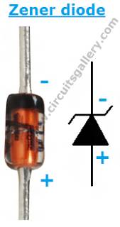
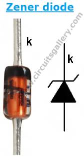
Do NOT use "+"and
"-"
to identify a zener. ONLY use the letter
"k"
Do not label a zener diode with "
98MHz OSCILLATOR
My first comment was this:
And a third reply:
Let's look at these comments and see how incorrect they are.
The circuit above oscillates. It has a coil and capacitor connected in
parallel to make a circuit called a TUNED CIRCUIT.
T.K. HAREENDRAN keeps emailing me about the mistakes on these
pages and hates to be criticised.
DOOR ALARM
The circuit DOES NOT WORK.
BATTERY CHARGER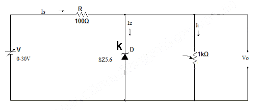
I know some readers think that one end is more positive than the other
when the diode is placed in a rectifying situation, but that reasoning
certainly does not apply in this circuit.
As you can see in the circuit above, the zener does not see "+"
on the lower lead, so "+"and
"-"
is not helpful - it is just CONFUSING !!!!!!!
![]()
![]()
You really need a cap across the coil to make a reliable osc.
The answer I got from a technician was:
The effective capacitor across the coil is the one from collector to
emitter.
And another answer:
Of course, there is a cap in parallel to the inductor.
As a consequence, we have a tuned circuit, which determines the
oscillator frequency.
The two capacitors are across the inductor with the battery in
series.
I made some comments about turning the transistor ON and OFF and get
this reply:
I think, it is not appropriate for this circuit to think in "ON" and
"OFF" terms. The circuit produces a sinusoidal output!
Then we have another comment:
The tuned circuit will have a Q value of maybe 100, in other words, the
circulating current will be much higher than the input current, this
will be built up over several cycles.
Firstly we need to look at the circuit and see if it oscillates.
![]()
This type of circuit produces a sinewave when connected to a power
supply and then instantly removed.
It does not need any other components and it does not need a transistor
to produce this effect.
So, what do all the surrounding components do?
They connect the TUNED CIRCUIT to the supply and quickly remove it.
It must be quickly removed, otherwise the voltage produced by the TANK
CIRCUIT will be reduced. In other words the surrounding circuitry will
put a load on the TANK CIRCUIT.
That means the transistor must be turned on and then turned OFF very
quickly.
This clears up the faulty thinking of one the replies above.
Now we come to the amplitude of the waveform produced by the TANK
CIRCUIT.
We are going to remove all the surrounding components and talk about the
TANK CIRCUIT.
For a correctly designed tank circuit, the energy stored in the coil is
equal to the energy stored in the capacitor.
This is necessary because the TANK CIRCUIT produces a waveform
consisting of half a cycle that is below the power rail and half a cycle
that is higher than the power rail.
For both these half-cycles to be identical, the component values must
match.
The full amplitude (called the peak-to-peak value) will be the addition
of these two values.
Q-values have nothing to do with current. They are a
voltage-determined value.
You can now see the first circuit does not have a capacitor across the
coil and even though some of the cycle may be produced by the
surrounding components, the equal parts of the waveform cannot be
produced.
We have not described how the TANK CIRCUIT produces a waveform above AND
below the power rail.
The easiest way is to remove all the surrounding components and tap the
TANK CIRCUIT across the battery.
This will put energy into the uncharged capacitor and it will be charged
to 3v. During this time the voltage will appear across the coil and it
will produce a small amount of flux that will oppose the voltage and
thus very little current will flow into the coil.
We are delivering energy to the circuit for a very short period of time
and this is too short for the coil.
Now the supply is removed and the energy from the capacitor is slowly
fed to the coil and it produces magnetic flux. The coil does not accept
energy any faster than a certain rate because the "applied voltage" -
the voltage on the capacitor, produces magnetic flux called EXPANDING
FLUX and this cuts the turns of the coil to produce a voltage in the
opposite direction to OPPOSE the incoming voltage and that's why the
capacitor discharges slowly.
So far we are producing the lower part of the waveform because the
bottom plate of the capacitor is at 0v and the capacitor is gradually
discharging.
The capacitor continues to deliver current until a point is reached
where the coil is producing a "back voltage" equal to the capacitor and
suddenly the capacitor cannot deliver any current.
The magnetic flux in the air surrounding the coil cannot be maintained
and it collapses. This produces a voltage in the turns of the coil that
is in the OPPOSITE DIRECTION.
We not have a situation where the voltage produced by the coil is
OPPOSITE to the previous voltage and as the magnetic flux collapses it
delivers a voltage to charge the capacitor in the opposite direction.
Since the two components are equally matched in "energy storage"
capability, the capacitor is charged to a voltage EQUAL to the original
voltage (but in the opposite direction).
Now you can see how the waveform rises to the voltage of the supply rail
when the capacitor has no charge and then rises ABOVE rail voltage as
the capacitor charges in the opposite direction.
This exchange could continue FOREVER but there are some losses with the
magnetic flux and each cycle becomes smaller and smaller.
If we have a transistor that delivers a small amount of energy at
exactly the right time during each cycle, the full waveform will be
maintained. That is what the transistor and surrounding components do.
For a 3v supply, the peak-to-peak value of the waveform will be 6v.
The "Q" of the circuit is 2. Not 100.
![]()
BACK LIGHT CONTROLLER
Here's another design from: T.K. HAREENDRAN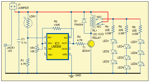
He claims to be a Professional Circuit Designer and "knows what he is
doing."
Here is a sample of his circuitry from Electronics For You
December 2015.
Look at the 22R resistors.
If you refer to
30 LED
Projects you will see an article on the importance of providing HEAD
ROOM for any string of LEDs.
Head Room is the voltage dropped (lost) in the current-limiting resistor
so that it "matches" the voltage across the LEDs and the supply voltage
to allow LEDs with slightly different characteristics to be used.
Every LED creates a voltage across its leads when it is illuminated.
This can be as low as 1.7v or as high as 3.6v, depending on the colour.
This is called CHARACTERISTIC VOLTAGE and varies very little if
the LED is small, medium or large. But it can change by as much as 0.4v
for white or blue LEDs.
But when you are connecting any number of LEDs to ANY supply, you need
to know the exact voltage that will appear across the LED when it is
illuminated.
This is easy to do. Just add a 100R or 470R and connect to 6v to
12v measure the voltage across the LED.
In a batch of LEDs, the voltage will vary from 3.4v to 3.6v and if 3
LEDs are connected in series, this will make a difference of up to 0.6v
for 3 LEDs.
The voltage for 3 LEDs can be from 10.2v to 10.8v.
If we have 3 x 3.4v on a 12vsupply, the voltage across the 22R will be
1.8v and the current will be 80mA.
But if the voltage of the LEDs is 3 x 3.6v, the current will be 55mA.
The author says the circuit can work with 3.4V/80mA, 10mm white LEDs or
with 8mm blue LEDs.
The data sheet states the 10mm white LEDs can be 3v to 3.4v. If 3
x 3v LEDs are used, the current through the 22R will be (12 - 9 = 3v)
3/22 = 136mA.
You can see the current will vary from 55mA to 136mA, depending on the
characteristic voltage of the LED and unless you test each LED very
accurately before using the circuit, they will be DAMAGED.
On top of this, the 12v must be an accurate 12v supply as an increase of
1v will will also damage the LEDs.
The idea of the CURRENT LIMIT resistor is to provide safety (prevent
over-current) for the complete range of possibilities that may occur -
including voltage rise.
22R only allows a range of 1.8v and this can be swamped by the supply
increasing by 1v and selecting a set of low CHARACTERISTIC VOLTAGE LEDs.
Using 3 LEDs does not allow very much HEAD ROOM and only 2 LEDs should
be used, unless you have accurately measured the voltages, and the
supply does not rise.
You can also get 10mm white LEDs that require 25mA max for 20,000mcd,
(10 cents each on eBay) so some LEDs are much more efficient than others
and much cheaper.
The other bad feature of the circuit is the rectangle for the LM358.
It should be drawn as an op-amp (a triangle) so you can instantly see
what is happening in the circuit.
![]()
Here is another junk circuit from Electronics For You
magazine August 2015.
It is a Door Alarm using a HALL EFFECT device.
If the output of IC1 goes to 0v, the emitter of T1 will be 0.6v due to
the base-emitter voltage of the BC557 transistor. The output transistor
will be turned ON all the time.
I can see this fault instantly. No-one in the technical department of
EFY picked up the mistake and published it to their 40,000 readers.
Every issue of the magazine has mistakes like this.
And they told me I could not "spot a mistake" in their magazine !!!
You don't need a complex circuit like this. Just a reed switch and a
magnet !!!
![]()
Here is another junk circuit from
Electronics For You
magazine August 2015.
It is a BATTERY CHARGER.
Why include a 7805 regulator when the 51R resistor will limit the
current to (30v - 14v = 16v) 16/51= 300mA or 30mA with the 510R resistor
(with the 7805 removed).
FUSIBLE RESISTOR
MOTOR CONTROL
The motor continues to operate about 2 seconds after the switch is
opened, until the 10u drops below 33% of rail voltage, as is discharged
via the 100k.
Here's some mistakes from Electronics For You Magazine January
2016:
The FET is in FOLLOWER MODE and this means the Source rises as the FET
turns ON.
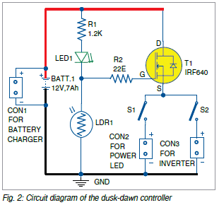
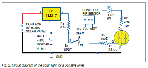
Why use a 450mA solar panel and then limit the charging to 180mA?
RGB Generator
The problem is the 100R on the tri-coloured LED.
PIR MOTION SENSOR
Here is another project from T.K. HAREENDRAN.
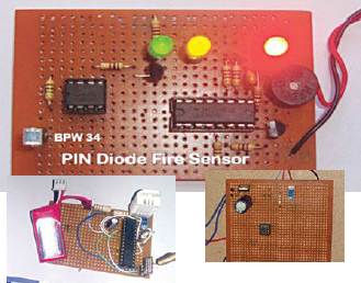
FIRE SENSOR
Here's another poor design from D. MOHAN KUMAR. All his
circuits are filled with mistakes. He has no idea how to design a
circuit.
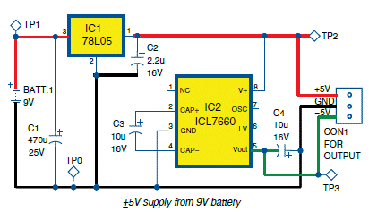
+5v -5v SUPPLY
Here is a project to produce 5v and -5v from a 9v battery for an op-amp,
or any circuit that needs a split supply.
3v3 ZENER
Let's look at the zener diodes and the current they can supply.
CONTROLLER
Here's another mistake from Electronics For You Magazine January
2016:
The load should be in the DRAIN. When the GATE is 4v to 10v higher than
the SOURCE, the FET turns ON and is finally FULLY TURNED ON.
METAL DETECTOR
The search coil consists of one turn and when you are picking up very
small magnetic fields, the voltage and current produced in the single
turn will be very small.
VU METER
Here is another project from Velleman.
The supply is 3v
LED TORCH
This is one of the worst kits I have seen from Velleman.
MOSQUITO REPELLER
This is a timing circuit from Mohan Kumar. None of his
circuit are designed correctly and this circuit has a BIG MISTAKE.
30 AMP POWER SUPPLY
If you want a 12v power supply at high current, the cheapest way is to use
a 12v rechargeable battery with a trickle-charge resistor.
But here is a question posted by a forum member.
Vidyasagar Sir�s Perfect Answers
Where is pin 6?
Vidyasagar Sir�s Perfect
Answers for HSC Board Exam,
www.vsagar.org
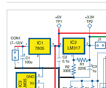
It would be much clearer to say the minimum output voltage of the LM317
regulator is 1.25v when pin 1 is connected to 0v .
SERIAL REGULATOR
The layout of a circuit is very important to prevent it being read
incorrectly.
NO PRINTED CIRCUIT BOARDS
Going through the last 12 months of Electronics For You you
find ALL the projects have been built on matrix boards and not one
project has a photo of the finished item on a Printed Circuit Board.
MAGNETIC GENERATOR
This is a SCAM.
This circuit looks to be suitable but you have to do the "maths" to see
how it will perform.
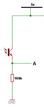
PHOTO TRANSISTOR
This circuit may or may not work. The hobbyist says it does not work.
The answer is to change the 10k for 100k.
The main problem with this circuit is the driver stage that turns on the
4 parallel 2N3055 transistors.
When the input goes HIGH, the base of the C1061 will be 2.1v above the
0v rail.
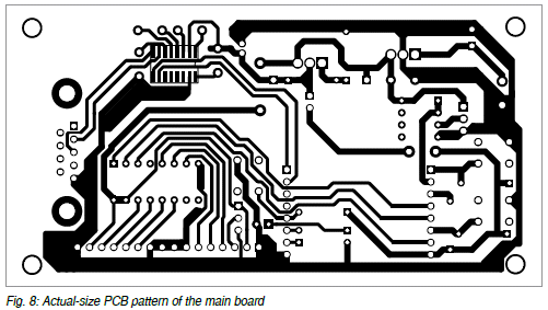
PCB PATTERN
Look at the outline of the IC. It is creating a short-circuit for all
the tracks going to the IC. It has not been removed from the trackwork
before publication. Just another sloppy bit of work from Electronics For You.
3-TERMINAL REGULATORS
There's two faults with this circuit from Electronics For You
April 2016.
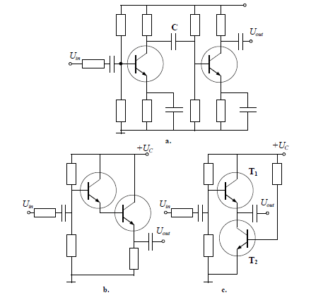
EMITTER-FOLLOWER
The output of an emitter-follower is
in-phase with the input. The red waveform in the circuit above
shows the correct output.
What
is the use of putting a circuit in a text-book without any values ????
It's only the values that will let you know what the circuit is doing
and how it is biased.
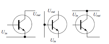
Look at this RUBBISH:
The centre figure is supposed to represent COMMON BASE configuration. If
I don't understand the circuit, how is a beginner going to understand it ???
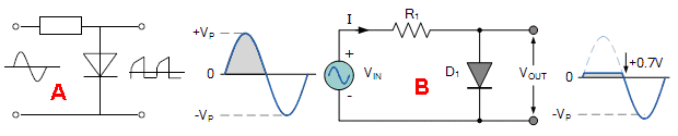
DIODE CLIPPER
The output waveform of diagram A is entirely
incorrect. See the output of diagram B. The max voltage will be 0.7v as
the diode turns ON at this voltage and when the waveform goes negative,
the diode is effectively "out-of-circuit."
Here is some of the terrible Engwish from: Feedbacks. The main toop to improve the frequency
response or the step response is a feedback.
FILTER
The whole idea of explaining how a Schmitt Trigger works is to show the
feedback from the second stage (transistor) to the first transistor.
This is shown in red.
Of course the author of the book has good intentions. But English is his
second language, however every page has left me wondering what he is
trying to say. Some of the statements don't make any sense AT ALL.
That's why I only use very simple English and don't try to show my
ability at use large, complex words and long, involved sentences. The
first time you use a long sentence, the reader will close the book and
put it on the shelf. You have lost him forever.
Page 11
Page 2
Page 3
Page 4
Page 5
Page 6
Page 7
Page 8
Page 9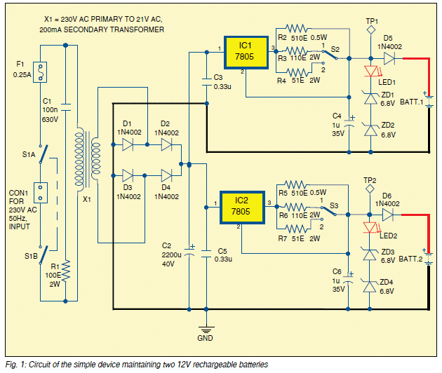
The 7805 simply maintains the current at 300mA.
The 2,200u is not needed and the 7805 is not needed.
Another over-designed circuit from
Electronics For You, making them look
stupid.
![]()
A resistor can be used as a FUSE, but it has one big problem. It creates
a voltage-drop across it and this means the supply rail needs extra
electrolytics to provide "stability."
One reader wants to replace an 82 ohm 0.5watt FUSIBLE RESISTOR.
An 82 ohm resistor will pass a current of 80mA and produce a voltage drop
of about 6v6 and stay warm for years, dissipating 0.5 watts of heat.
The current needs to rise by at least 50% for the resistor to start to
fail and in most cases it will fall off the board before it changes
resistance or the leads will create a dry joint.
When the current increases by 50% (120mA) the wattage (heat) generated
will be over 1 watt and the resistor will fail.
However it will go up in smoke if a short-circuit occurs and then you
will have to find the shorted component.
If the resistor is replaced by 82R 0.75watt, it will take about
1.5watt to burn out and this will be about 140mA and the voltage across
it will be about 10v to 12v.
A 0.75 watt can create a lot of heat and fire if burning out slowly, so
it must be covered with fibre-glass tubing and kept away from the PC
board and all other components. ![]()
Here is a circuit that can be simplified: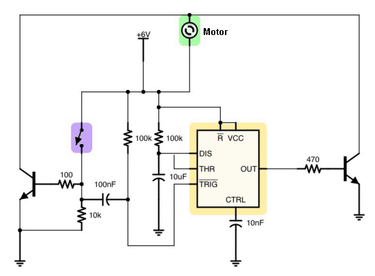
I have mentioned it before. When designing a circuit, see if the design
can be simplified, as someone will always come up with a simpler design.
That's the skill in designing a circuit. And that's the skill we are
showing you in these articles.
We are beyond any text book or university course. We show you more than
just being able to design a circuit. We show you how to simply it and
improve it.
There are lots of businesses that have gone broke when a competitor has
brought out a cheaper and simpler design. The Garrard turntable, tape
recorder, video recorder, transistor radio, TV and lots of mechanical
devices.
It takes a very clever person to see a device and say: "I can simplify
this!"![]()
But the Gate must be about 2v to 4v HIGHER than the Source for the FET
to be fully turned ON.
This means the Source can only rise to 8v to 10v.
The reason for using a FET is the very small voltage dropped across the
Drain-Source terminals when it is fully turned ON and that's why it is
able to pass a high current.
This is another useless circuit by Bikash Rai that has not been checked
or tested by the non-existent technical staff at Electronics For You.
![]()
Buy a 200mA panel and remove the LM317.
![]()
When the red LED is turned ON, pin 2 will be HIGH and the voltage across
the LED will be 1.7v.
When the green LED turns ON, it needs 2.1v and only 1.7v is available,
so I don't know what will happen.
And when the blue LED turns on too, it requires 2.3v and I have no idea
what will happen.
The common cathode of the tri-LED should be connected to 0v and 100R's connected
between each
of the anodes and the outputs of the chip.
This will allow each colour to be driven correctly.
In other words, the tri-coloured LEDs are around the wrong way !!!
Here is a comment from Andrew:
Have a look at the switches and resistors (R4-R7) on Port 1 pins. Since
the AT89c2051 has (approx) 50kohm internal pull-ups on Ports 1 and 3,
the Indian 'designer' didn't actually need to add these extra four 1k
resistors. However, having done so, he tied them all to ground! If they
had been connected to Vcc, the switches could have been read. The way
the circuit shows, the resistors are not effective. The port pins are
tied to ground via the 1k resistors and the switches connect to ground
when pressed. What a mess !!!
![]()
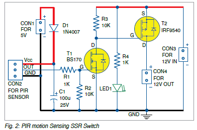
Here are 4 points to improve this circuit:
1. The PIR module works on 5v to 20v. A separate 5v supply is not needed.
The PIR can be connected to the 12v rail.
2. A 1N4007 diode is not needed as the module only consumes 3mA !! Use a
signal diode 1N4148.
3. BS 170 costs 70 cents. A BC547 transistor can be used (cost: 10
cents)
4. R1 is not needed.
![]()
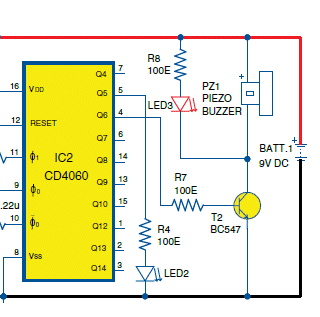
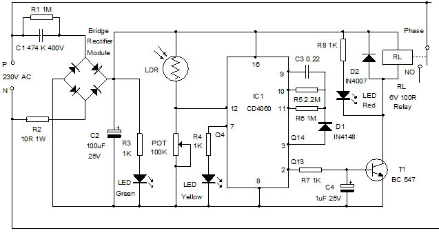
The CD 4060 IC can deliver about 10mA from each of the outputs. If
you try to take more than 10mA, the output does not go fully HIGH but
drops to an unknown value while delivering about 10mA (or slightly
more).
This puts added strain on the output and shows the author of the circuit
is not a good engineer.
In the circuit above, the 100R resistors on the output will try to take
80mA, and this shows the incompetency of the person designing the
circuit. A LED only needs 10mA and a transistor only needs a few
milliamp.
The output will only deliver about 10mA, but the output voltage will
only be a few volts due to the low value of the load resistor.
If this circuit was presented in any magazine, other than one from
India, the author would never be allowed to supply another project.
It is obvious Electronics For You has no-one to test or check any
of the projects and that's why the magazine is filled with RUBBISH like
this. ![]()
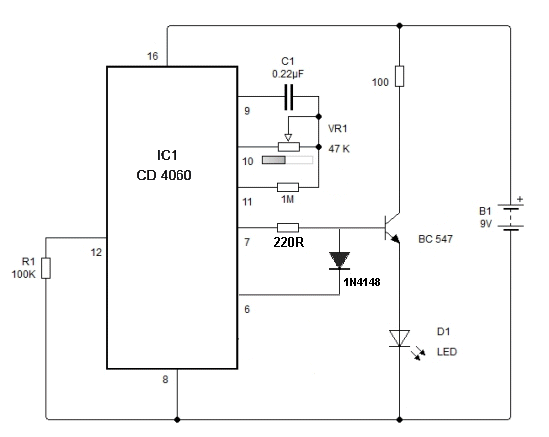
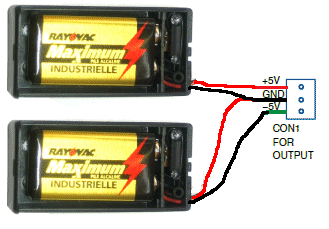
The simplest way to do this is to use two 9v batteries (or AA cells to
produce 6v). The circuit below does not need a switch and is not
limited to 50mA per output. It is also much cheaper. This is the art of
thinking OUTSIDE THE SQUARE.
It is easy to produce something
extravagant and expensive, the skill is to produce something simple and
cheap.
![]()
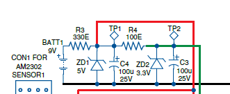
What happens is this.
The zener diode passes (loses - wastes) a certain amount of current via
the load resistor and when you draw current from a ZENER REGULATOR
CIRCUIT you actually take (rob) the current from the zener.
The first zener regulator circuit consists of a 5v zener and 330R. The
voltage across the 330R will be 4v and the current through the resistor
will be 12mA.
You can only take up to 12mA. If you try to take more than 12mA, the
"stable" 5v drops to a lower value.
In other words, the circuit DROPS OUT OF REGULATION.
The second ZENER REGULATOR CIRCUIT is the 3v3 zener and 100R. The
voltage across the 100R will be
5v - 3v3 = 1.7v. The current through the 100R will be 17mA.
But we only have 12mA available !!!!
This means the 5v zener regulator circuit will DROP OUT OF REGULATION
and the 5v will drop below 5v BEFORE the project is connected to the
supply !!!!! The voltage will drop EVEN FURTHER when the circuit is
added (connected).
This circuit has obviously NEVER been tested and SOMNATH BERA has
no idea how to design a circuit.
Just another untried, untested circuit from Electronics For You.
This problem can be detected very quickly by simply looking at the
component values. It does not need a University professor to sit down
for 30 minutes and work out the values. You can do the calculations "in
your head" in 30 seconds and that's what I am getting across in these
pages.
You have to carry out quick calculations for everything you do, so you
don't make a fool of yourself.
Every project in Electronics For You has mistakes. I have
notified "Chopra" for the past 2 years and he has done nothing to
correct the situation.
In fact he has omitted all my corrections in subsequent issues. He only
talks about "R1" should be "R2" and other similar nonsense.
![]()
But since the FET is in FOLLOWER mode, the source rises if the FET turns
ON and the voltage on the gate never rises above the voltage on the
source.
The following two diagrams show how the FET should be connected in a
circuit:
![]()
Here is the front end of a metal detector. The search coil
consists of a loop of 1 turn and is fed into a transformer
consisting of 1 turn. The other winding is 75 turns.
The circuit was designed by non-electronics personnel and we will
explain the problem: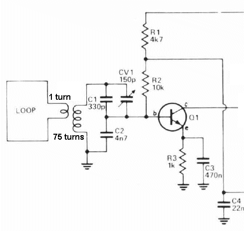
The transformer connected to the loop consists of 1 turn and 75 turns
and theoretically the output voltage will be 75 times higher than the
voltage generated by the loop.
But the current will be reduced enormously and we all know a transistor
is a current-controlled device, and a considerable current is needed to
get it to work, especially when 10k is connected to the base.
The circuit will be much more sensitive if more turns are added to the
"loop" and the output is connected directly to the transistor.
![]()
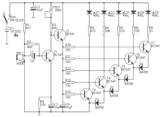
The supply is 3v and the final LED has a voltage drop of 1.7v across it
when illuminated. The drop across each diode is 250mV = 1v and the
collector-emitter voltage of the final transistor (T7) is 200mV.
This makes a total of 2.9v.
Here is a graph of the voltage when 23mA is flowing:
You can see the voltage falls below 3v after a short time and it will be
very difficult to illuminate the top 3 LEDs.
The circuit is a very bad design as no allowance has been made for the
battery voltage to fall (as the battery get older).![]()
It is a LED torch using a 12v lighter battery. This battery has 8
very small cells with a capacity of 55mAHr.
The blurb claims the battery will last 10 hours but LED1 will take 38mA
when the battery is fresh. Firstly, this is too much for a LED and
the battery will last less than 1 hour.
When the battery voltage drops below 8.5v, the two white LEDs and red
indictor LED are illuminated. I don't know why this has been done but it
makes the LEDs illuminate very dull when the battery is low. ![]()
The 474 capacitor on the input will deliver 30mA and the main load in
the circuit is the 1k and green LED. This means the supply voltage will
be about 30v. This voltage is too high for the chip and it will be
damaged.
In actual fact we don't know what the supply voltage will be as the chip
will start to draw current and the supply will drop but we don't know
the final voltage.
A 6v 100R relay draws 60mA at 6v, but we only have 30mA available, so we
don't know what will happen when the transistor turns ON.
It's just a stupid circuit with no known operation conditions.
You cannot drive this type of circuit from a capacitor-fed power supply.
![]()
If you want high current for a long period of time, use a larger battery
(car battery).
High current power supplies have enormous problems, mainly due to the heat they
generate (waste) and the danger of one transistor short-circuiting and
delivering 30v to the equipment you are powering.
In the circuit above, more than 500 watts will be wasted as heat when 30
amps flows and this will be like a small radiator bar.
You only build a circuit (make a project) when it is economic and
reasonable. If there is a cheaper alternative (such as a ready-made
power supply), it is better to get the guaranteed performer.
Electronic construction only came about 80 years ago, because products (such as radios, CB radios and amateur radios were not available, or were very
expensive).
It's wonderful to learn about electronics, but if the cost of building
it yourself is 3 times the cost of a ready-built item, you have to weigh
up the economics.
The output voltage of the 24v transformer is too high as it will deliver
30 volts after the bridge and the circuit only needs 18v for it to
operate fully. It needs a 16v transformer and these are not readily
available.
That's why a project like this requires a lot of decisions before you
commence construction. It also needs an enormous amount of heatsinking,
and this is expensive. 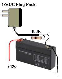
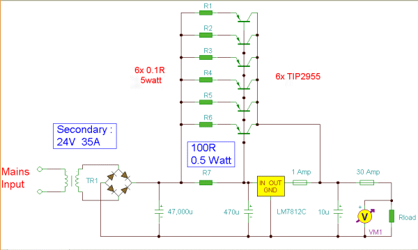
He wanted to replace the TIP2955 transistors with MJ11015 Darlington
transistors.
He asked if the 200 watt dissipation MJ11015 transistors would
work better than the 90 watt dissipation TIP2955 transistors.
There are a couple of points to note, before giving an answer.
The voltage on the output of the bridge is 30v and the output voltage is
12v. The difference is 18v and the current is 30 amps. This
produces 18 x 30 = 540 watts of wasted energy.
It does not matter if the wastage is though resistors or any type of
transistor. The heat being lost is 540 watts.
Each transistor will dissipate 90 watts and this is the maximum for a
TIP2955 transistor.
But don't forget the MJ11015 transistor is almost identical and to think
it will dissipate 200 watts is stretching reality.
Both transistors will get extremely hot and you will need a heatsink
300mm x 300mm to keep them cool.
Just because the MJ11015 transistor is capable of dissipating 200 watts,
does not mean it will be a batter performer.
Both transistors are likely to short-out under these conditions and I
would never run a transistor to its maximum temperature. You are only
asking for trouble.
The only difference between the two devices is the base current.
The MJ11015 transistor will require only 1% of the base current and the
7812 will run much cooler. ![]()
Here is his silly explanations of the 555 pins: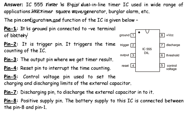
Pin 2 triggers the chip when the voltage is less than 33% of rail
voltage. He does not say that.
Pin 7 discharges the capacitor to the negative rail. You
don't say: "into the pin."
Pin 8. The supply is not always a battery.
We don't say "counting" for a 555 chip. We leave the word
COUNTING for chips that COUNT
![]()
Here is his poor explanation for the LM317 3-terminal regulator: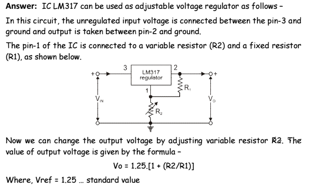
As the resistance of R2 is increased, the output voltage passes down R1
and creates a voltage across R2 that "jacks-up" the regulator and the
output voltage rises. The output voltage is always 1.25v higher than pin
1 and the regulator can be "jacked up" to nearly 35v. Now I
understand what is happening.
![]()
You may think the circuit above has a good layout, but when you see the
improved layout below, you can see the output of the transistor has been
drawn closer to the 0v rail to emphasis the relative voltage levels.
It might be a small matter but all these things help to make a circuit
easy to understand.
![]()
Even though many projects have a PCB layout in the magazine, none of
them have had a board created and loaded with components.
Electronics For You
is the largest electronics magazine in India and NONE of the projects
have been finalised and proven successful.
Every other magazine in the world takes a photo of the finished design
and offers boards to the constructors who want to build the project. But
not Electronics For You.
Here's a prototype from Electronics For You April 2016:
This is the sort of quality presented in the largest electronics
magazine in India !! A junk board with hand-writing on the top of
the board. I would not have this sort of junk in my work-room, let alone
send it off to a magazine. Look at the resistor and jumper at 45
degrees!!! Electronics For You is just an embarrassment.
![]()

It uses the good name of Tesla in an attempt to pretend he invented a
motor-generator type of set-up that produces electricity without any
energy entering the system
This is called OVER-UNITY and so-far no-one has created such a device.
However they claim over 10,000 investors are already powering their
houses with the "device."
No-on has an open-house to show their apparatus. No-one has a video and
no news organisation has interviewed anyone with a demonstration. It's
just waste of $49 for the .pdf
Here's the .pdf
TESLA'S SECRET $49.00 !!
and here's another fraud:
RUN
YOUR CAR ON WATER $69.00 !!
![]()

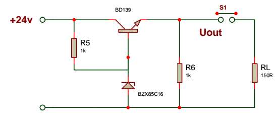
To start with, the two 13v zeners will have a "dead spot" of 2v because
they add up to 26v for the 24v supply.
On top of this the base-emitter junctions at the top and bottom will add
another 1v.
This means the input voltage will not have any effect when it is rising
and falling by 3v because this is the "gap" between turning on the
bottom zener then the voltage falling and turning on the top zener.
Normally "biasing diodes" are just at the point of turning ON, so the
rising or falling signal will pass through the diode, even when it is a
few millivolts.
Any voltage below 3v will not be transferred and a 5v signal will have
some attenuation in the 1k as well as the 2u2. Most 5v signals
from a digital source are less than 5v as the output of most chips is
4.5v max and 0.5v min. This gives a 4v p-p signal and the other two
losses makes this circuit very unreliable.
On top of this, zeners have a 5% tolerance and another 1v may disappear.
This circuit is called an AC AMPLIFIER.
It only amplifies when the signal is rising or falling. When the signal
is a minimum, the 2u2 starts to charge via the top 13v zener and the
emitter-base junction of the top transistor.
It charges to 10v. When the signal rises to 5v, the right-side of the
capacitor should rise to 15v, but at 13.6v the zener is turned ON and
the base-emitter junction is active. This means only 1.4v of the 10v is
removed.
When the input signal goes to zero, only 1.4v is replaced in the
capacitor.
That's the first fault.
The second fault is the amount of time taken for the capacitor to charge
and discharge.
The charging will be very quick because the charging resistor is 1k.
It will take MUCH LESS than one second to charge and discharge.
When the input signal is 1Hz, the circuit will react in less than 100mS
and for the rest of the time the output will be zero.
Thus the circuit is not designed for low frequencies.
This is one example of a circuit designed by an "electronics engineer"
who did not put enough thought into the design. Before you publish
anything, build the circuit and test it thoroughly. This way you will
not release something that dos not work.
![]()
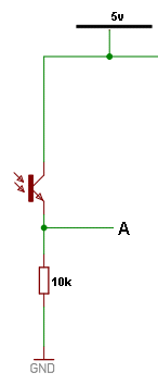
ORIGINAL CIRCUIT
Let's see why:
The circuit is a simple VOLTAGE DIVIDER.
The voltage at "A" will be 2.5v when the photo transistor has a
resistance of 10k.
The voltage at "A" will be 4.5v when the photo transistor has a
resistance of 1k.
The hobbyist needs a voltage of 3.5v but the photo transistor needs a
very bright light to achieve this voltage.
IMPROVED CIRCUIT
The voltage at "A" will be 2.5v when the photo transistor has a
resistance of 100k.
The voltage at "A" will be 4.5v when the photo transistor has a
resistance of 10k.
The photo transistor has a resistance of less than 10k in normal light
and the circuit will now work.
![]()
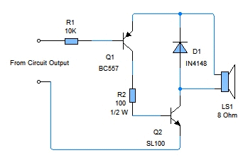
PUSH-PULL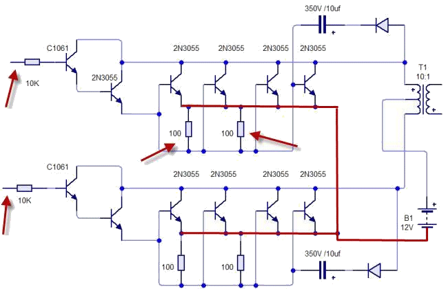
When the 4 transistors turn ON, the collector voltage will drop to a
very small value.
But the collector voltage of the C1061 cannot fall below the emitter
voltage, otherwise the transistor will not deliver a current via the
emitter. 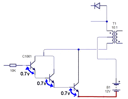
When the 3rd transistor turns ON, the collector cannot fall below about
2v because the collector of the C1061 must have a voltage above the
emitter for current to flow. This means the voltage across the 4 x 2N3055
transistors will be at least 2v and they will not be fully turned ON. ![]()
![]()
A 3-terminal regulator needs about 2-3 across it for reliable operation.
You can get low-dropout regulators to replace the "old-style" regulators
and they have a lower dropout (350mV to 1v or so).
In the circuit above, the 7805 needs 2v across it and if the input
voltage falls below 7v, the circuit will not work properly.
The LM317 needs 1.7v and only 1.6v is available. Use low drop-out
regulators for both these regulators for reliable operation.
![]()

When R2 = 0, the current amplifier is a voltage repeater because the voltage
gain is equal to unit.
Besides stabilizing of transresistance, the inverting feedback has the same
benefits as the non-inverting voltage feedback that is decreasing distortion and
output offset.
Conventionally, energy approaches electrical end electronic systems from the
power generators of different types: hydro, wind, and heat generators, atomic
stations, etc.
Summary. A power supplier has to meet the requirements of the energy
consumer, which needs the
determined power, voltage, and current values and shape. Voltage sources supply
fully controlled voltage,
whereas the current may be unpredictable. Current sources generate adjustable
current flow, whereas
the voltage may change during the supply process. In practice, there is neither
the pure voltage nor the
exclusively current sources, but one of the features is predominant.
Passive low-pass filters. A low-pass filter reduces high-frequency
particles of a signal and passes its
low-frequency part.
Nevertheless, in power circuits, they function as the protective devices for the
load under the shorts.
High frequency signals pass through a capacitor because the waveform on
the left plate rises and falls very rapidly and this makes the waveform
on the right plate rise and fall at the same rate and the capacitor does
not have time to charge and discharge.
A high frequency signal appearing on the top of a coil produces an
opposing voltage from the coil that prevents the energy in the waveform
entering the coil and passing to 0v - because the opposing voltage has
the same amplitude and prevents the waveform passing through the coil.
It is exactly like walking on a swimming pool filled with corn starch.
https://www.youtube.com/watch?v=D-wxnID2q4A
If you
run very quickly across the pool you will not sink into the corn starch
solution.
But if you stop, you will sink.
If the signal is low frequency, the opposing voltage from the coil has a
low amplitude and the waveform passes through the coil (because it has a
very low resistance).
It is the desire of all designers to achieve accurate and tight
regulation of the output voltages for customer
use. To accomplish this, high gain is required. However, with high gain
instability comes. Therefore, the
gain and the responsiveness of the feedback path must be tailored to the
adjusted process. ????????
SCHMITT
TRIGGER
Normally the first transistor will produce a change on the collector
when the input changes by about 0.7v This is normal transistor
action in a common-emitter circuit. This means a small input
signal will change the output. In fact a change of as little as 100mV
will affect the circuit. But when we have a feedback line as in this
circuit, the operation is completely different.
Suppose the input waveform contains noise of 100mV. This noise will affect
the output in a normal amplifier.
To prevent it affecting the circuit we increase the distance between
the low and high trigger points to say 3v.
This "gap" is called the HYSTERESIS GAP.
The circuit below has values to emphasize how the input works.
Suppose the first transistor is turned ON. The voltage between the
collector-emitter terminals will be less than 700mV (about 300mV) and the second
transistor will be OFF. The second transistor sees 300mV between base
and emitter and it will be turned OFF.
The voltage across the 4k will be 8v and the voltage across the 1k will
be 2v.
The voltage on the base of the first transistor will be 2.7v
To turn the first transistor OFF, the voltage must be reduced.
When it is reduced by 100mV, the first transistor begins to turn OFF and
the voltage on the collector rises. This turns ON the second transistor
and the current through the two 1k resistors produces a voltage across
the lower 1k. This raises the emitter voltage and although the base
voltage DOES NOT RISE at this point in time, the voltage between the base
and emitter of the first transistor is REDUCED. This turns OFF the first
transistor and this is done without the input voltage changing. It is
the SWITCHING ACTION of the two transistors that cause the circuit to
change states.
The two transistors continue this action until the first transistor is
completely turned OFF and the second transistor is completely turned ON.
This action is called REGENERATIVE ACTION and means the action continues
within the circuit without any external influence.
The circuit finished up with the voltage across the top 1k as 5v and across the lower 1k
as 5v.
The base is still at 2.6v The first transistor is completely OFF and the
second transistor is completely ON.
To turn ON the first transistor the input signal has to rise to 5.7v
This is a 3.1v rise and we have changed the circuit from 0.7v detection
to about 3.1v detection.
The important fact to remember is the circuit creates the rapid
switching action and NOT the input signal and the gap between HIGH and
LOW is about 3v.
The signal shown in red is called a FEEDBACK signal.
It is a POSITIVE FEEDBACK signal because it assists the input signal in
performing its intended task.
With a feedback signal, you cannot consider a signal that is of the same
polarity as being positive.
The signal is really ASSISTING (helping); or HINDERING (opposing) and
can be rising or falling and yet ASSIST the incoming signal.
You are not trying to show how clever YOU are. You are trying to
get a complex point across by saying it is really very simple to
understand.
![]()
Page 10
Page 11
Page 12
Page 13
Page 14
Page 15
Page 16
Page 17
Page 18
Page 19
Page 20
Page 21
Page 22
Page 23
Page 24
Page 25
Page 27
Page 28
Page 29
Page 30