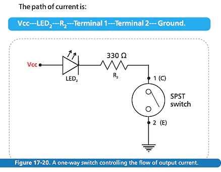
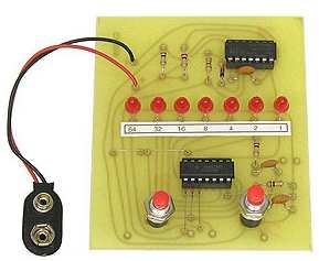
SPOT
THE MISTAKES!
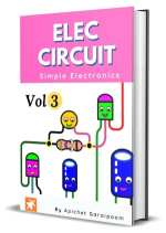
Page 34
Page 1
Page 2
Page 3
Page 4
Page 5
Page 6
Page 7
Page 8
Page 9
The circuit above takes 9mA all the time via the middle 1k
resistor and the LED takes 8mA when it is illuminated.
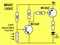
The improved circuit takes 2 microamp when light falls on the
Light Dependent Resistor and the first transistor is turned OFF. This makes it
"disappear" from the circuit and all we have is two 10k resistors connected
between the base and emitter of the PNP transistor and these turn the transistor
OFF. So nothing else in the circuit is taking any current. A huge saving on
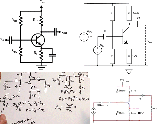
current. COMMON EMITTER
AMPLIFIER
To make a long story short . . . In 50 years I have never used any of the
internet mathematics to design a circuit. It is not relevant and does not apply.
It is remote from what is needed and does not take into account external
influences. It is a complete waste of time putting pen-to-paper. But telling the
"Professors" is a waste of time. Nothing has changed. I sent my concepts
to all schools and colleges in Australia, over 40 years ago and got no reaction.
I explained that the only way to learn electronics was through building
projects. Not one school or University bought a single kit in 40 years.
The reason . . . . when the project did not work . . . because of
student incompetence . . . . the instructor did not have the skills to fix it in
front of the student. It's as simple as that. The blind leading the
blind. Talk is CHEAP. Blabbering in front of blackboard
is easy. Proving your blabberings is difficult.
CHINESE SOLDER
2 LAMPS
Page 10
Page 11
Page 12
Page 13
Page 14
Page 15
Page 16
Page 17
Page 18
Page 19
Page 20
Page 21
Page 22
Page 23
Page 24
Page 25
Page 26
Page 27
Page 28
Page 29
Page 30
Page 31
Page 32
Page 33
Page 34
Page 35
Page 36
![]()
Electronics is such a big topic.
I have produced lots of articles to try
and cover the subject and maybe covered 1%.
Text books are filled with useless circuits and mathematical questions that I
have never come across in 50 years of designing modules.
All the things you want to know are missing from text books. That's because the
writer has never designed a circuit in his life or fixed any faults or problems.
The same with University Professors. Students come out of a $70,000
5-year course and never soldered a resistor!
One University student applied for a job at my business and said "Oh, I don't do
any soldering."
Remember this: When you come out of your 5-year course, the interviewer will ask
you for your experience . . . you have none.
That's why you have to start NOW and have electronics as your hobby and take
projects to the interview to distract the interviewer from asking awkward
questions. ![]()
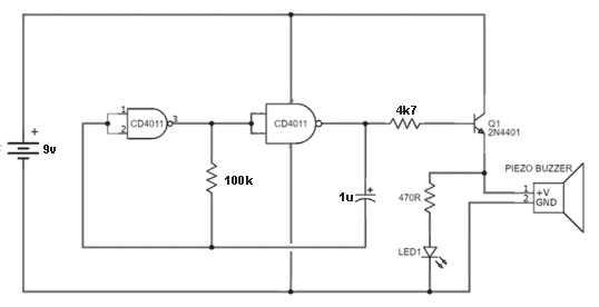
NIGHT LIGHT
Here is a circuit from the web, from an "engineer" who doesn't understand
circuit design. He claims the "circuit works" and that makes the circuit a good
design.
But if you look at it carefully, the circuit takes the same current when
operating as when it is resting. This is a waste of battery-current. And the
circuit takes DOUBLE the necessary current.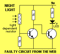
![]()
YouTube is filled with instructional videos explaining the Common-Emitter
amplifier and similar related circuits.
Most of these demonstrations are quite impractical, as they use component-values
that I have never seen in reality and none that I would recommend.
But more important, you have to "look outside the box" and understand that you
cannot design a circuit without knowing the characteristics of the input signal
and the impedance of the stage that is connected to the output.
You cannot specify a signal that comes from a sinewave generator as it is
completely different to that found in a normal circuit.
In fact there is nothing you can specify or predict, as the results will be
completely different to reality.
It is absolutely pointless going into the fine detail of including base-emitter
voltage drop and using a value of 100 for the gain of a transistor as you are
finishing up with a "dream" value for the stage.
Even learning the fundamentals of knowing how to find the gain of a stage is an
unnecessary exercise as it will bear no resemblance to the actual value.
I have never used a mathematical calculation in my life as I know it produces
NOTHING.
University students are being led "up the garden path" with questions and
computations that are just a waste of time.
But a University cannot charge $70,000 and tell the student to build the circuit
and measure the results. So they have to lull the student into false sense
of achievement by complicating the issue with mathematics. It's a SCAM. And
after the COVID lockdown, a lot of the University myths have been uncovered and
debunked. Even Elon Musk has mentioned the ineffectiveness of University
teachings. In some areas they are effective as no student has the technical
equipment to carry out medical operations, but in many another areas he has said
the only way to learn is on-the-job.
And the fastest way to learn is called REVERSE LEARNING. A medical student
learns the fastest when he attend a dying heart patient and sees how the
operation is carried out. An electronics person learns more by diagnosing a
faulty device and seeing how to locate the fault.
![]()
Don't buy Chinese Solder. I have bought 10 different types from China and
none of them worked. For some, I had to increase the temperature and the solder
still did not stick. For others, the solder poisoned the tip of the iron and I
had to remove all the solder and apply Australian solder.
I don't know what is wrong is wrong with the Chinese solder as some was 63/37
and is supposed to be low melting solder. None of the solder gave a nice shiny
result and I have now stopped my experimentation. It was just a waste of
time and money.
The only way I could use-up the solder was to twist the rubbish with my good
solder and melt the two at the same time and my good solder would make a result
that I could use.
I have written a lot more on solder and soldering on:
Here is the article.![]()
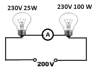
For a start, you have to know the characteristics of a filament globe. The
resistance of a globe is about one-sixth when it is cold and it increases six
time when it is fully illuminated.
This means it takes 6 times more current to get it to start to glow. If you
cannot supply this current, it will never start to glow.
We are not going into any mathematics because we don't have to.
The 25 watt lamp will only allow a small current to flow in the circuit and this
will be less than 25% of the current needed to get the 100 watt to start to
glow. Thus it will never start to glow and its resistance will always remain
low.
Now we look at the 25 watt globe. The supply is 200v and it is a 230v globe. So
the supply is on the low side.
Now we look at the effect of the 100watt globe.
It has a resistance of about 25% of the 25watt lamp so the initial voltages
across the lamps will be divided into 5 parts with 4 parts across the 25watt
lamp and one part across the 100watt lamp. This puts 160v across the 25watt
lamp.
We now have to find out if the lamp will start to illuminate. Only a
demonstration will show this.
After it starts, the resistance of the 25watt lamp will increase, whereas the
resistance of the 100watt lamp will remain the same and thus the 25watt lamp
will see a higher voltage and maybe it will glow brighter.
![]()
ELECTROLYTICS
Here is a very simple circuit called a Capacitor Discharge Unit.
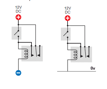
When the switch is in the down position, the 2,200u electrolytic is charged and the solenoid pulls the core into the solenoid. This is because the core is a magnet. When the switch is in the up position, the core is pushed out of the solenoid. This is because the current flows in the opposite direction.

You would think the strength of the activation is
the same in both directions, but when the switch moves into the up direction,
the 2,200 is directly across the solenoid. And the full voltage of the
electrolytic is passed to the solenoid.
However when the switch is down, the 2,200 is charged via the power rail and
since the initial current is very high, the power rail will not be able to
deliver this high current and the voltage will dip.
To reduce this dip, two 1,000u electros have been added, but we come to a
technical situation where a 2,200u electrolytic is taking energy from 2,000u
storage and if the 2,200u electro has zero voltage across it and the other has say 24v,
the instantaneous initial voltage will be just 12v across each. That's why the
impact in one direction is not as strong as the other.
![]()
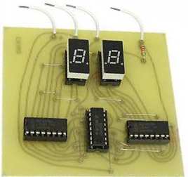
PCB

What a terrible Printed Circuit Board artwork to put in a magazine. Many of the lands are touching nearby tracks and you could not make the board without creating lots of mistakes.
The secret is to firstly keep all components away from other items and when you are going to place a track through the pins of an IC socket, the width of the track is reduced.
In addition, the value of the components must be included on the overlay as you might be making the project 2 years after the board is manufactured and you will never remember the values.
All my 1,000 PC boards are fully labelled so they can be assembled years later without having to reference to any other information.
This is just a sign of professionalism. Something I have not seen in any magazine, website project or any product on the web. Even the indicator LEDs needs to be identified so you know how to read the output of the project.
I was the first person in the world to put good quality Printed Circuit Boards on the cover of my magazine when the other magazines had no overlay, no tinned lands and no solder mask. Just a paper-bakelite piece of rubbish.
These are things you need to know to turn you into a quality engineer and real expert.
The board above is not labelled, I don't know what it does.
I went to an electronics shop 50 years ago and they had hundreds of unlabelled boards. It is no wonder none of them were sold. They were all just junk.
![]()
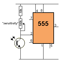
TRANSISTOR INPUT IMPEDANCE
![]()
A BC547 transistor identifies as a common NPN transistor with no special features and almost any NPN transistor can be used.
Both resistors have very high values to show the effect of this demonstration.
We are commonly told the input impedance of a common-emitter stage is 2k, 5k, 10k or some other low value.
But the input impedance varies enormously according to the collector current.
When the collector current is very low, the base will respond to an extremely small current, in the order of a microamp or less. In the circuit shown, the transistor turns ON fully with a 10 meg base resistor. This is one microamp base current.
This means you have no idea of the sensitivity of a stage and when you are detecting very small currents. The input (wires) will have a high impedance and this will make them susceptible to interference such as hum and spikes. You will need suppression-capacitors to reduce this noise. (not covered in this discussion)
In summary, we are saying a transistor has a very high sensitivity (very high input impedance) when detecting microscopic input currents and this impedance will fall dramatically to 2k or less when the transistor is operating at maximum collector current.
In other words, a microscopic base current will not drive a LED or motor or globe or any other high current component in the collector circuit. The collector load can only deliver about 200 times more current than you are delivering to the base.

You can increase the input impedance by connecting
one transistor on top of another. This is called CASCADING.
This will increase the input impedance by a factor of at least 200. And when you add
another transistor the impedance is increased by another 200 times.
This produces an enormously sensitive circuit and the diagram on the left will
detect static electricity.
![]()
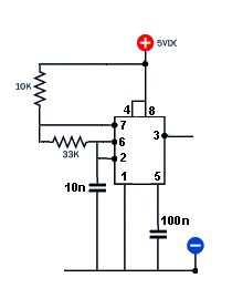
555 IC MISTAKE


The whole idea of drawing a circuit is to present the components in the simplest
way possible.
The original circuit has been improved but the placement of the 555 pins is not
ideal. However the major mistake is connecting a 470u directly to pin7. This pin
has a low-current transistor inside the IC that "shorts-to-ground" and the
energy in a 470u can blow-up the transistor.
![]()
ELECTRONICS MAKER MAGAZINE

India's second largest electronics magazine has ceased providing construction
projects in the magazine.
Why do they keep the title ELECTRONICS MAKER if there is no "maker" in the
magazine.
A few years ago I provided them with articles for 18 months and did not get one
single reply from any of the 40,000 subscribers. That's not-one-in-720,000
views.
India is just fooling itself with slogans like: "Make in India."
I don't know where the fault lies, but the University lecturers on the web have
very little understanding of basic electronics and what is needed to be taught.
They just fill the whiteboard with mathematics and equations and come with up
with answers that are far more accurate than the data !!!
I have never seen them explain how a circuit works, and certainly no mention of
how to test it.
And now the magazine does not have any articles for the beginner or the
constructor.
They are just allowing China to take over the field. And they are. China
is designing many electronics items and they show enormous skill in programming
and buying microcontrollers that are only available to the Chinese market, for a
price that is one-tenth of our purchase price.
The Western World needs electronics engineers to design products because the
Chinese do not know what we want or how to design things aesthetically.
Unfortunately everything is going "down-hill" and China is rising.
However the recent downturn in China-economics has seen millions laid-off and
more than 10 million apartments either abandoned or unfinished with millions of
purchasers unable to reside in their unfinished dwellings.
And this is only the beginning of the collapse.
![]()
UNDERSTANDING THE 555 IC
The circuit shows an IR transistor connected to pin 2 of a 555 IC.
Technically the 555 will trigger when the voltage on pin2 is lower than 33% of
the supply voltage.
But there is no resistor supplying a voltage to pin2. The 555 will react when
the voltage on pin2 is lower than 33% of rail voltage as there are some
resistors inside the chip that cause the chip to start-up in a "set-mode" but
you cannot use them in your designs.
When the Infrared light is turned off, the chip requires a HIGH on pin6 to
change state but the voltage on pin2 must be above 66% of rail voltage to this
to occur, as pin2 controls the action over the voltage on pin6.

The solution is to place a high value resistor between pin2 and the supply rail.

The IR transistor creates a voltage divider with this resistor and we call this
a HIGH IMPEDANCE or LOW IMPEDANCE SET-UP, depending on the value of the
resistor.
If the resistor is 10k, we can say it is low-impedance, because this is a
low-value for this type of set-up.
It will require a high level of IR light to change the state of the 555.
On the other hand, a 100k will produce a high-impedance input and the 555 will
respond to a very low level of illumination. This is called sensitivity. The
following circuit shows a sensitivity pot with a 10k "stop resistor" to prevent
damaging the transistor.
Pin6 needs to be connected to a resistor or switch to complete the circuit.
![]()
COMMON EMITTER STAGE
![]()
Too much time and effort has been put into describing and analysing the Common
Emitter Amplifier.
The facts are these: The gain of a transistor can be anywhere from 150 to 450
and it is a waste of time producing a mathematical result for the gain of the
stage.
The gain will depend on the impedance of the stage connected to the output and
if this is unknown, nothing can be calculated.
However the mistake in the circuit above is the biasing.
You cannot connect the base to the supply rail. If you replace Rb with an
adjustable resistor, you will find the collector voltage is equal to the supply
voltage and as you decrease the resistance, it will immediately fall to nearly
zero.
You have no opportunity to set the collector voltage to mid-rail and thus the
output voltage will be "clipped" or "bottomed."
In other words it will be distorted and this type of circuit is useless for a
demonstration. In fact it is useless for anything.
![]()
TIMER
We have covered lots of faulty circuits from Mr Mohan Kumar as he
does not test any of his designs and most of them do not work.
The main problem with this circuit is the 10k resistor on the base of the T2.
This will allow very little current to flow and depending on the resistance of
the relay. It may not "pull-in." The resistor should be 1k to 2k2.
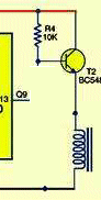
The circuit has been simplified to a transistor,10k and relay so you can
see the mistake.
Here is how to instantly work out what is happening.
The transistor will have a gain of 100. It might have a gain of 330, but when a
small current or medium current flows, you can only allow a gain of 100.
The transistor divides the 10,000 ohm resistor by 100 and the transistor turns
into a 10,000/100 = 100 ohm resistor.
The supply is 6v and we have a 100 ohm resistor in series with a 5v relay.
Suppose the relay needs 100mA to operate. Its resistance will be 5/.1 = 50
ohms. We have 100 ohms in series with 50 ohms and 2v will appear across
the relay. Obviously, this will not work. If the relay requires
50mA, the resistance will be 5/0.05 = 100 ohms and the relay will see 3v.
You can instantly see this circuit will not work reliably.
That's how you see all EMITTER FOLLOWER circuits.
Here is a voltage regulator circuit using an EMITTER FOLLOWER. It is a
Power Supply that takes a higher voltage and converts it to a lower voltage,
depending on the value of the zener diode.
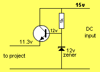
It is also called a SERIES REGULATOR (to distinguish it from a SHUNT REGULATOR
arrangement).
The point we are making is this: How much current will the circuit pass?
The only thing that is taken into account is this: The transistor will have a
gain of 100 and it will convert into a 1,000/100 = 10 ohm resistor.
If you draw 100mA, the voltage across the transistor will be 0.1 x 10 = 1v.
If you draw 300mA, the voltage drop across the transistor will be 3v and if you
draw 400mA, the drop will be 4v, but you don't have 4v available !!!
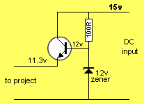
Here is the circuit with 100R base resistor. The voltage across the resistor is
3v. The current through the resistor will be: 3/100 Amp = 30mA. The
transistor will multiply this current by 100 = 3Amp.
The other way to look at the circuit is this: The transistor will turn into a 1
ohm resistor. You have about 3v available between 11.3v and 15v. 3 amps
flowing through a 1 ohm resistor produces a voltage drop of 3v.
Both methods come to the same conclusion. But you have to know the
current-handling capability of the transistor and the power supply.
![]()
REVERSE VOLTAGE
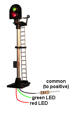
Many of the 2-aspect signals come with a 1k current limiting resistor to
allow the signals to operate on 3v to 12v. Make sure you never allow a LED to
see a reverse voltage above about 5v as it will be instantly destroyed.
A resistor of 470R in the common line will prevent excess current flowing if you
make a mistake.
![]()

A new "club" was promoted on Jameco website, where beginners can join for $19.99
for a 12 month subscription. But when you fill out the application, the
charge is $99,00 A typical "bait and switch."
The site is filled with technical mistakes and diagrams:
The main fault with the diagram above is this: A switch is placed on the
EARTH RAIL. Imagine if all the lights in your house were wired like this.
They would all still be "live" when switched off !!
A lot of the wording is not common terminology: "Glowing a LED"
Preset?? . . . . should be "mini trim-pot."

Continuity Test of of an LED !!! (proof-reading needed.)
We don't talk about "Continuity of a LED." We talk about the
characteristic voltage drop due to the colour.
![]()
AMERICAN KITS
I was sent an email recently
with a link to an American supplier of educational kits for beginners.
What I found was a total disaster.
The Printed Circuit Boards had no overlay, no tinned lands and it looks like they had been hand-made with tape, some 20 years ago. They were single-sided
with lots of links,
What I am complaining about is this. In this "day and age," to deliver rubbish
like this to hobbyists is unfathomable.
What are they trying to present?
I am not blaming the supplier. He does not have any intelligence or any
understanding.
I blame the teachers for accepting this rubbish and not forcing the supplier to
improve his product.
I go back 50 years when the Chinese produced rubbish like this and responded to
complaints.
Over a period of time they improved and now stand as the worlds foremost
producer of acceptable electronics.
This reinforces my statements of the educational standards in the USA.
I was on my own with saying their standards were the worst in the world, but I
have been backed-up recently.
The cost of a degree or diploma or "Masters" is astronomical for the "product" it
provides.
I have seen the courses, the content and was staggered by the lack of content
and training.
Not one course covers the skill in soldering. Not one course mentions
TIP-CLEANING PASTE and not one course explains how to remove a component.
Not one course explains how a transistor really works and not one course explain
ANYTHING understandable to designing the simplest circuit.
This is because the "Professor: has never designed a circuit in his life and
certainly never repaired 35,000 electronics devices, like I have.
One University graduate came to me for an application and said: "Oh, I don't do
soldering."
And another said: "When I design a circuit, it will work." I asked,
"Where did you get that idea from?" "That's what the University
Professor told us."
It's called MESMERISM.
Fooling the student into thinking has has an understanding of electronics, just
because he has paid $70,000.
Look at the links and the lack of component values
Another "Junk" board
What does it do?
Look at this quality kit from Aliexpress
America is crying: "Why are we
failing? You only have to look at the underlying state of the Education.
China is producing kits for half the price and 10 times the quality of American
suppliers.
But don't be surprised. I have contacted Universities, manufacturers, magazines
and kit suppliers. Not one has replied.
![]()
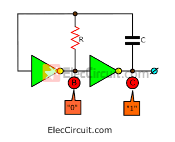
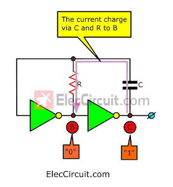
DISCHARGING A CAPACITOR
I have included a number of circuits from the web to show that it does not
matter how the circuit is constructed or the type of gate (NAND or NOR).
The point l want to make is this.
How does the capacitor get discharged?
No one has covered this point and it does not matter until you need to describe
how the circuit works.
That�s the position l was placed in before l started my magazine
TALKING ELECTRONICS.
Things don�t matter until they matter.
It seems such a trivial point.
But a capacitor has to discharge so that it can charged for the next cycle.
Ideally, it discharges fully.
To discharge fully, both leads have to be at the same potential. They can both
be at 12v or 0v. In other words, the capacitor can be discharged while �high� or
discharged while at zero voltage.
And the thinking is this: The input of a CMOS gate has a very very high input
impedance (resistance), so how does any capacitor connected to it, discharge?
Here�s the secret.
As soon as the voltage on the input rises above the supply voltage, a diode
connected to the input, and also connected to the power rail, is activated and
the voltage cannot rise above the supply voltage.
This diode is only active when the input line is higher than the supply.
Otherwise is does not do anything.
Obviously you cannot put a
high voltage on the input as it will immediately flow through this tiny diode
and the current will destroy the diode. However the current from the discharging
capacitor does not damage the diode.
This is how the capacitor discharges. One lead cannot rise above the supply
voltage and if the other lead rises to this voltage, the capacitor sees equal
voltage on both leads and discharges.
It�s as simple as that.
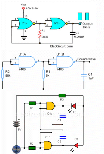
BEEPER CIRCUIT
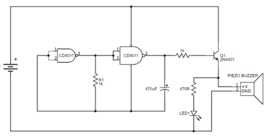
Not only does the BEEPER circuit have a mistake, but the component values are
incorrect for CMOS gates. The value of 1k and 470u are related to TTL gates
where the input impedance was much lower and had an effect on the charging and
discharging of the capacitor.
CMOS devices have input impedances that are 1,000 times higher and it is
intelligent to use values that reflect this. The capacitor should be from 100n
to 1u and the resistor from 100k to 1M
These values show you have an understanding of what you are presenting.
The corrected Beeper Circuit is shown below:
When the circuit is turned ON, the electrolytic will
be uncharged and the output will be unknown.
Say it is HIGH. The input will be HIGH and the join of the two gates will be LOW
and this will make the output HIGH.
If it is LOW, the input will be LOW and the join of the two gates will be HIGH
and this will make the output LOW.
The 100k will try to charge the 1u in the reverse direction and it will start to
leak when the voltage rises and may not charge. So the capacitor has to be
non-polar (a ceramic) or a lower value ceramic.
So, this circuit WILL NOT WORK.
RUBBISH
Here is a whole lot of incorrect information:
The problem is this:
The part of the cycle he is describing is the DISCHARGING of the capacitor. And
it does not discharge via the resistor. But via the input of the first inverter.
But he knows nothing about the diodes on the input of the gate and thus he
should not be writing on the web.
All the rest of his discussion is completely incorrect.
Also he does not understand the fact that a gate changes state when the input
voltage is slightly higher and slightly lower than mid-rail voltage. It does not
have to rise to 100%. Maybe something like 30%, 70%.
I will take up where he has started. The capacitor is fully charged and the
output rises. As it rises, it delivers a voltage to the input that is higher
than the supply. A protection diode on the input of the first gate will not
allow the input to rise higher than the supply, so, as the output rises, the top
of the capacitor "hits a ceiling" and will not rise. So it gets discharged via
the protection diode. Now the output is HIGH and the input is HIGH.
It would stay like that all day if it were not for the resistor. The resistor
CHARGES the capacitor, because the bottom lead of the capacitor is HIGH and the
bottom of the resistor is LOW.
As the capacitor charges, the voltage on the input of the first gate reduces and
when it fall to about 30-40% of rail voltage, point B goes HIGH. This makes the
output go LOW and the whole capacitor drops by a voltage equal to rail voltage.
The input voltage had about 30% rail voltage on it and now the voltage drops by
full rail voltage.
This means the input voltage will drop below 0v, but a protection diode on the
input prevents it dropping below 0v, so the input just goes to 0v and the rest
of the voltage on the capacitor is quickly removed.
Now the output of the first gate is HIGH and it begins to charge the capacitor
via the resistor and when the voltages reaches about 60% of rail voltage, the
two gates change state to start the next cycle.
Note: the capacitor has times when it is partially charged and discharged very
quickly via the protection diodes.
This has never been mentioned in any discussion. Everyone thinks it is a "smooth
cycle."
![]()
SPIKES
A customer bought a capacitor discharge unit and it worked for one day.
I don�t know what failed but he said the BD679 transistor failed due to spikes
from the solenoids.
There is a lot of misunderstanding about how spikes are generated from
inductors.
The only time a spike is generated is when the current is turned off. This
causes the magnetic flux to collapse.
If the inductor is supplied from a capacitor and the energy from the capacitor
gradually reduces, there is no rapid �turn-off� of the current and thus no
collapse of magnetic field and thus no spike. The magnetic field simply reduces
slowly and the energy in the magnetic field is delivered to the metal core.
Since there is no spike, a reverse-biased diode is not needed.
The customer stated:
As an electronics engineer, I believe that this failure is because there is no
diode protecting the transistor from the large negative spikes that will be
generated by the solenoids.
There should be a diode
connected across the output terminals (reverse biased) which would protect
against negative spikes from the solenoids.
As an electronics engineer, I believe that this failure is because there is no
diode protecting the transistor from the large negative spikes that will be
generated by the solenoids..

When one of the push-switches is pressed, the energy from the capacitors drives
the double-acting solenoid and the voltage falls very rapidly to a few volts.
When the switch is released, the solenoid is no longer connected to the circuit
and so no back emf can enter the circuit.
![]()
MAKE
Make is a website containing a lot of electronics for young enthusiasts.
It has projects, magazines, books and kits.
But it is not really technical and does not explain electronics in any detail or
accuracy.
I have not challenged them because there is almost nothing of any value.
The kits are overpriced and I saw a 555 IC on a matrix board to produce two
flashing LEDs.
The kit price was $9.00 and shipping $28.00 !! You can
buy the same thing on Aliexpress for 72 cents on a nice Printed Circuit Board !
The author of MAKE Electronics emailed me about me providing a copy of one
of his books on my website for the past 12 years for FREE.
I said the book contained an enormous number of mistakes and mis-descriptions of
components and a lack of understanding how components worked.
He asked me to send him a list of the mistakes, which I did.
Here is just a few of the mistakes and you can see how the author lacks the
understanding and knowledge to be competent to present an electronics book to
beginners.
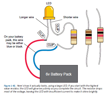
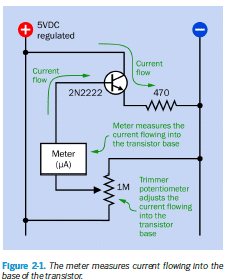
Here is the first picture in the book. It has a major mistake. When the pot is turned fully, the LED will blow up. The resistance of the potentiometer will be very close to zero and a high current will flow and damage the LED. You must have a "stop resistor" in series with a pot to prevent excess current.

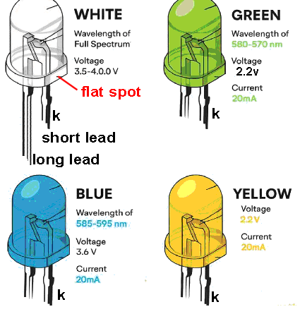
Here is a description of the LED with very little detail.
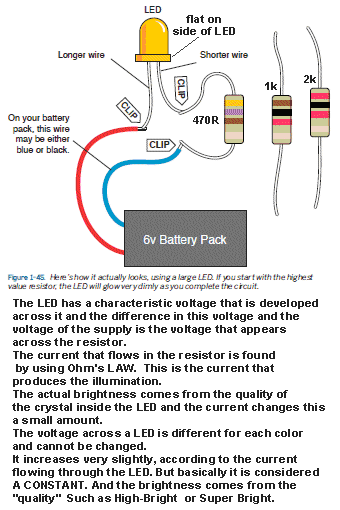


Fig:2 is the "ACCEPTED" way to draw a diagram.

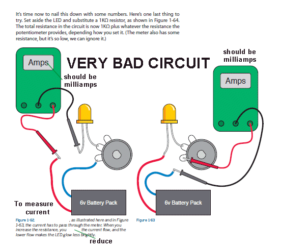
How Big a Resistor Does an LED Need?
Suppose that we�re use the Vishay LED. Remember its requirements from the data sheet? Maximum of 3 volts, and a safe current of 20mA. I�m going to limit it to 2.5 volts, to be on the safe side. We have 6 volts of battery power. Subtract 2.5 from 6 and we get 3.5. So we need a resistor that will take 3.5 volts from the circuit, leaving 2.5 for the LED. The current flow is the same at all places in a simple circuit,
This is an absolutely absurd discussion.
You have no control over the characteristic voltage that a LED develops.
I have explained how the voltage across the LED and resistor is determined and produced.
This paragraph should be removed from the book immediately.

NO. The
meter measures the voltage between emitter and ground (0v).
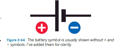
This is not a BATTERY symbol. It is the symbol for a CELL.


These are 2 bad diagrams because a single cell will not illuminate a
LED and the second diagram does not have a limiting resistor.
I don't know how you magically think this circuit will work.
The clapper does not move from one contact to the other. It just "jitters' or
"vibrates."
And secondly you will find the back emf of the coil will damage the LED.

I have never read so much rubbish in my life
These are three normally closed switches. SHOW THEM AS n/c SWITCHES
What does the 1k do???? Nothing. Go through the circuits and
determine if each component is needed.
I don't know where you get "+" and "-" symbols from, but we are
not talking about a DUAL POWER SUPPLY.
I have never seen this rubbish before, in my life.
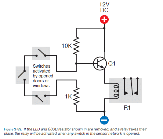
Figure 3-91.The self-locking relay
depicted has been incorporated in the alarm circuit, so that if any switch in
the network is opened, the relay will continue to power the noise maker even if
the switch is closed again.
SELF-LATCHING

The book has only LAYOUT DIAGRAMS. You need
to include a schematic.
I have no idea how the circuit works unless all the components are placed in
their
recognised positions.
That's why I can "see" a schematic "working" instantly.
The value of the components MUST be included.
That's why only technically competent people should be in charge of producing
technical material.
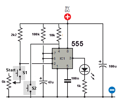
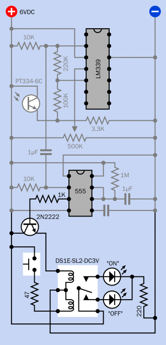
Here is the circuit correctly laid out as a schematic.
Here is the description from the book:
The 2k2 holds the trigger (pin 2) positive until S1 is pressed,
which lowers the voltage depending on the setting of the 5k potentiometer. When the
trigger voltage falls below 1/3 of the power supply, the chip�s output (pin 3)
goes high for a period determined by the values of the 100k and 47u. S2 resets (zeros)
the timer, by reducing the voltage to pin 4, the Reset. The 100u smoothes the power
supply, and the 100n isolates pin 5, the control, so that it won�t interfere
with the functioning of this test circuit.
The 5k pot is not needed as the switch just has to reduce the voltage in pin 2
to below 33% of rail voltage and if the pot has a low value or zero ohms, it is
not needed.
Here's how the circuit works.
Pin3 and pin7 have the same "state." When pin 3 is LOW, Pin7 is low and
the 47u is being discharged. When pin 3 is HIGH, Pin7 is HIGH and it is really
"out of circuit" so the 47u can be charged via the 100k.
When the "Start" Sw is pressed, Pin2 goes LOW and pin 3 goes HIGH to illuminate
the LED and Pin7 "disappears from the circuit" to allow the 47u to start the
charge.
When pin6 sees 66% of rail voltage, the 555 IC changes state and pin 3 goes LOW
and Pin7 goes LOW (discharging the 47u).
This is called the TIME DELAY of the circuit.
Sw2 is not needed as the 555 does not have to be "reset."
![]()
MAKE - More Electronics
The author continues his terrible diagrams in this
book.
If I can't follow and understand how a circuit or diagram works, how do you
expect a beginner to understand it?
Terrible layout
This is the way the circuit should be laid out. When you write an electronics
book, you don't put the components anywhere on a diagram. Every component
has a specified location. That's how everyone can read them and understand.
Current flows from the top of the circuit, into the base.
In addition, the authors circuit does not have a "stopper resistor" and when the
pot is turned fully, the micro-ammeter will be damaged and the transistor will
blow-up.

terrible layout

The correct layout of the components
The author said: You have to be careful to install the
phototransistor the right way around. Here�s the rule:
Positive current enters a
phototransistor through the short lead, and exits through the long lead.
What RUBBISH. The leads on a photo transistor are the same length.
The case will look like an ordinary transistor and the data sheet will show
c,b,e. Never go by lead length for transistors. There is no protocol
for lead-length.

Almost all transistors will be E, B, C.
This is just a jumble
This is the correct lay-out
No text book, YouTube video or University course has clearly
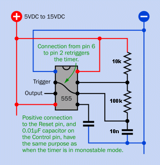
explained how a 555 IC works.
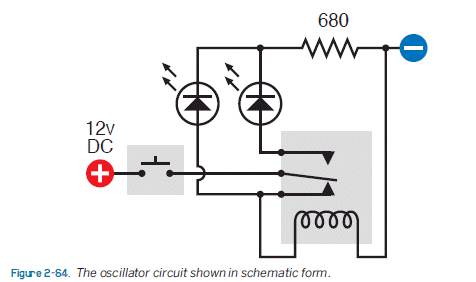
The circuit above is a "free-running" oscillator . . . . . called SQUARE
WAVE OSCILLATOR or running in ASTABLE MODE.
The thing you have to remember is this: Pin7 and Pin3 are HIGH and LOW at the
same time.
The only difference is this: Pin3 will drive a LOAD when it is HIGH and
also when it is LOW. The load has to be connected between pin3 and either the
supply or 0v. In other words it will "sink" or "source."
Pin7 will only "sink" when it is LOW. In other words, Pin7 will have 0v on it
when it is LOW.
When it is "HIGH" it disappears from the circuit. This is when Pin3 is HIGH.
Pin 2 controls the chip.
When the voltage on Pin2 is LOW, the 555 IC is turned ON and pin 3 goes HIGH.
At the same time Pin7 goes HIGH and disappears.
This allows the 10n to charge via the 10k and 33k.
When the voltage on the 10n reaches 66% of rail voltage, Pin6 detects this
voltage and turns the chip OFF.
Pin3 goes LOW and so does Pin7.
Pin7 stops the 10n from charging (because we say it is "shorting to deck") and
it now discharges through the 33k.
When the voltage on pin2 reaches 33% of rail voltage, the chip turns ON again.
The chip turns ON and OFF between 33% and 66% on the 10n.
Pins2 and 6 have nothing to do with the charging or discharging. They are
just high-impedance detectors for the 555.
Pin7 just creates a "link to ground" or "short-circuit" during the part of the
cycle that discharges the 10n.
I have
no idea how this circuit works. You will just have to re-draw the circuit
to align with the conventional way, to see what is
happening. The secret behind its unusual operation is the 47u connected to pin5.
By adjusting the voltage on this pin, the ON-OFF timing of the circuit is
altered. This alters the sound.
Build the circuit and see the effect. The 10u is an electrolytic and
should have the positive connected to pin 3 and the other one with the negative
connected to "-".
Even the numbering of the pins should be shown as I found a book with the
numbering around the wrong way.
The circuit above delivers only a few milliamp to the surrounding components.
The 555 IC is cheaper, but the choice is yours.

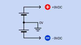
Voltage divider discussions show the supply at the top so the beginner can see
the increasing voltage "as a picture" and not have the decipher the diagram.
For simple examples, if the top resistor is the same as the bottom resistor, the
voltage is half-rail-voltage.
If the top resistor is half the bottom, you have three "halves" and one-third
the voltage is across each portion,
The other two are the same.

Figure 2-9. Emitter voltage varies almost linearly with base current, in a 2N2222 transistor. This graph was derived
from numbers in the table shown previously.
You are describing an EMITTER FOLLOWER circuit and this type of circuit is
rarely used. Maybe 1% of the circuits.
This discussion is pointless and I have never used it in 50 years.


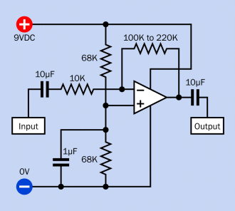
The circuit should be turned so the positive is the top rail and the op-amps
inside the chip shown on the diagram so you can see what is happening.
The "crossing wires" should also be clearly identified as "not touching" as you are catering for
beginners.

You can fix-up this circuit by making the 1u into electrolytics, the 220 into
220R, clear-up the crossing wires and re-draw the 555 so it is understandable.
Until this is done, I have no idea how the circuit works.
I see only one input of the op-amps connected to the circuit and I don't
see how the op-amps can produce a guaranteed output.
Show me a circuit in a text book where only one input of an op-amp is connected
!
Of course you can get a circuit to work with "mystery" floating voltages, but
this book is supposed to be EDUCATIONAL.
The author has concentrated on emitter-follower designs and this is a very bad
policy, as
the author is not an electronics person.
The 555 does not output "rail-to-rail" It is about 1v less than the
rail and can be up to 1.5v less.
When the 555 is HIGH, the output voltage is less than 5v. Then you have a slight
drop across the 1k resistor and finally a base-to-emitter drop of 0.7v.
This gives the relay less than 4.3v
A Common Emitter stage will drop less than 0.5v.
That's why you have to understand electronics before diving into producing a
book.
The relay must be Panasonic DS1E-SL2-DC3V relay. These cost $11.50 plus $24.00
delivery from DigiKey!!!
With intelligent designing you can get a 5v relay from Aliexpress for $3.00 and
$5.00 shipping. Or a 3v relay for $3.60 with $7.00 shipping.
4k7 is far too low and will over-stress the FET and produce "bacon-and-eggs" crackling noise.

All these absurd values shows the author has has no experience
in designing circuits.
The coupling capacitor is far too
Try and work out the power supply connections!!
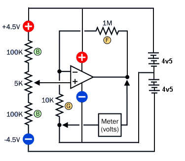
I had to draw the split battery to understand how it is connected to the op-amp.
This is a diagram of two cells. How do you get 18v out of 2 cells?
This schematic shows the lack of understanding of audio signals.
You don't need 10u on the input. 100n would be sufficient.
10u on the output needs to be a polarised (electrolytic).
The "rule of thumb" is to use 10n on the input and 100n on the output.
Or 22n on the input and 1u on the output.
Or
100n on the input and 10u on the
output.

You are going to get almost no volume from the speaker with 100R
series resistor. Maybe 8%.
I have already mentioned all the other mistakes.
A transistor operates on current. Why is he talking about voltage?
An increase in Current to the base will change the voltage on the collector
You can get a huge change in voltage on the collector and the voltage on the base may change by only 50mV.
A transistor is a CURRENT amplifying device.
oooooooooooooooooooo0000000000000000ooooooooo
Capacitors
47pF, 68pF, 100pF, 0.0001μF, 0.01μF 0.033μF, 2.2μF
The author has jumbled up his capacitor identification and made a mistake!
47pF, 68pF, 100pF, 0.0001μF, 10n ,
33n, 2.2μF
All the rest of the projects in the book
are constructed on prototyping board.
0.0001μF =
100pF !!! . . . . . Maybe he means 10n. That's why you
don't use these old-fashioned identifications.
Remember this: .001
= 1,000
so that 0.001uF = 1,000pF = 1n and 0.0001uF = 100pF
But the circuits are so complex that
I would not bother to "make" any of them. (Note the "pun.")
Page 1
Page 2
Page 3
Page 4
Page 5
Page 6
Page 7
Page 8
Page 9
In 50 years of creating projects I have always provided a Printed Circuit Board.
You learn nothing by fitting jumpers and wires and links down rattley holes that
produce noise.
All my 350 kits have IC sockets so the IC's can be removed if you think you have
damaged something.
It costs $3.00 extra to provide a quality Printed Circuit Board with all the
parts labelled on the top, tinned solder lands and plate-through holes.
The author is "dreaming" if he thinks a beginner can put this circuit together.
The whole book is "half-baked" with mistakes galore and enormous difficulty in
working out what the circuits do.
They do not follow "circuit-convention" and if I have not learnt anything from
this book, the beginner will just be led "down the garden path."
![]()
Page 10
Page 11
Page 12
Page 13
Page 14
Page 15
Page 16
Page 17
Page 18
Page 19
Page 20
Page 21
Page 22
Page 23
Page 24
Page 25
Page 26
Page 27
Page 28
Page 29
Page 30
Page 31
Page 32
Page 33
Page 34
Page 35
Page 36